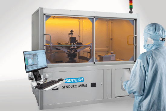
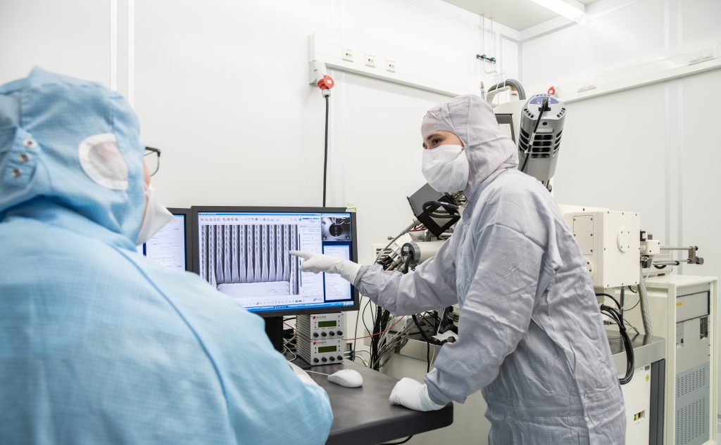
Plasma Process Technology
Thin Film Metrology
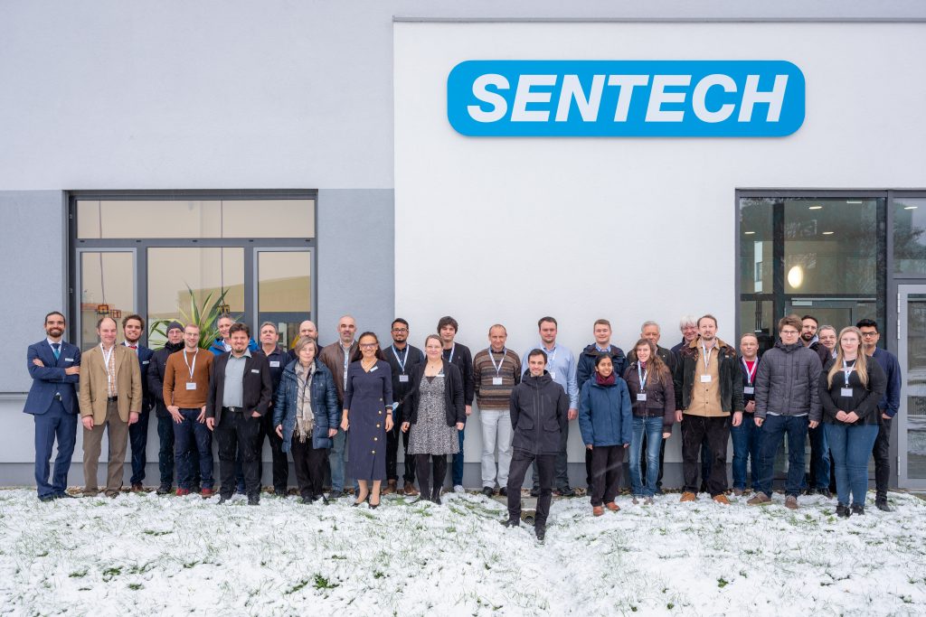
Read about the latest company news and product developments from SENTECH.