Laser Ellipsometry
Understanding Laser Ellipsometry and Why This Precision Technique is Important in Thin Film Metrology for Semiconductor Research
Laser ellipsometry is a non-destructive optical technique used to measure thin-film thickness and optical constants (n and k) by detecting minute changes in the polarisation state of light upon reflection. In semiconductor research, where nanometer- and even Ångström-scale control over materials determines device performance, laser ellipsometry has become a vital tool. It enables precise monitoring of thin films such as oxides, nitrides, and photoresists used in advanced integrated circuit fabrication and material development.
Learn more about the SENTECH range of laser ellipsometers, or scroll down to understand why this is an important thin film characterisation technique in semiconductor device research.


Why Use Laser Ellipsometry?
The increasing complexity of semiconductor devices demands ever-tighter control of layer thicknesses and material properties. Laser ellipsometry stands out among metrology techniques because it is:
- Highly sensitive: Capable of detecting sub-nanometer changes in thickness.
- Non-destructive and contact-free: No risk of contaminating or damaging the wafer surface.
- Self-referencing: Since ellipsometry measures the ratio of reflected light components rather than absolute intensity, it maintains excellent repeatability and stability.
- Comprehensive: It can extract both film thickness and optical constants simultaneously, providing insights into composition and density variations.
These capabilities make laser ellipsometry indispensable in both research and process control, particularly in the fabrication of transistors, dielectric stacks, and optical coatings.
How Does Laser Ellipsometry Work?
At its core, laser ellipsometry measures how polarised light changes after reflecting from a sample surface. The technique records two parameters, Ψ (Psi) and Δ (Delta), which describe the amplitude ratio and phase difference between p- and s-polarised light components. Mathematically, this is expressed as:
[
\rho = \tan\Psi,e^{i\Delta} = \frac{r_p}{r_s}
]
where ( r_p ) and ( r_s ) are the complex reflection coefficients for p- and s-polarised light, respectively.
By comparing the measured Ψ and Δ values with theoretical predictions from an optical model of the sample, researchers can deduce both film thickness and complex refractive index.
Because the measurement depends on polarisation changes rather than intensity, ellipsometry offers extremely high precision, even for ultrathin films below 10 Å. Advanced versions, such as spectroscopic ellipsometers, extend this principle across multiple wavelengths and angles to characterise multilayer structures, graded materials, and anisotropic coatings.
When and Where Is Laser Ellipsometry Used?
Laser ellipsometry finds application throughout the semiconductor value chain, from fundamental materials research to high-volume manufacturing. Typical use cases include:
- Process development: Optimising thin-film deposition (ALD, CVD, PVD) and oxidation steps.
- In-line metrology: Monitoring wafer uniformity and detecting process drifts in production environments.
- Research and failure analysis: Studying new materials, surface treatments, or degradation mechanisms.
- Optoelectronic and photovoltaic devices: Measuring anti-reflective coatings, transparent conductors, and passivation layers.
Its combination of accuracy, speed, and non-destructive measurement makes laser ellipsometry one of the most trusted metrology techniques in both fab and R&D settings.
Advantages in Semiconductor Workflows
- Sub-Ångström Sensitivity: Laser ellipsometers can detect thickness changes smaller than 0.1 nm, crucial for advanced gate oxides and high-κ dielectrics.
- Rapid, Repeatable Measurements: Measurements take only seconds, allowing for statistical process control and wafer-to-wafer consistency monitoring.
- Comprehensive Data: Unlike reflectometry, ellipsometry provides both thickness and optical constants, helping engineers detect variations in film composition or density.
- Model-Based Analysis: Optical models can incorporate multilayer stacks, roughness, and graded interfaces, improving fit accuracy and process insight.
Addressing Measurement Challenges
While powerful, ellipsometry is inherently model-dependent, the accuracy of results depends on how well the optical model represents the real structure. Incorrect assumptions about layer order or material properties can lead to ambiguous thickness results.
To overcome this, modern systems employ multi-angle measurements or combine ellipsometry with reflectometry. These hybrid configurations remove ambiguity and extend the measurable thickness range to several tens of micrometres. Additionally, advanced data analysis software can simultaneously fit multiple wavelengths and angles to ensure robust, reliable results.
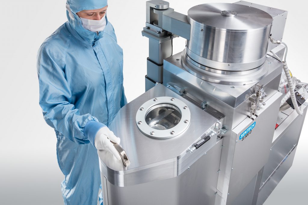
The SENTECH SE 400adv is a precision laser ellipsometer designed for rapid, high-accuracy thin-film characterisation. Using a stabilised He-Ne laser and multiple incidence angles, it delivers sub-angstrom resolution and excellent measurement repeatability.
The SE 400adv is ideally suited for semiconductor, optical coating, and photovoltaic research laboratories that need compact yet powerful metrology tools. Its high-speed data acquisition and automated operation make it well-suited for both process development and routine quality assurance.
Key features include:
- Multiple fixed measurement angles for enhanced sensitivity.
- Robust mechanical design for long-term stability.
- Intuitive software for model creation and batch analysis
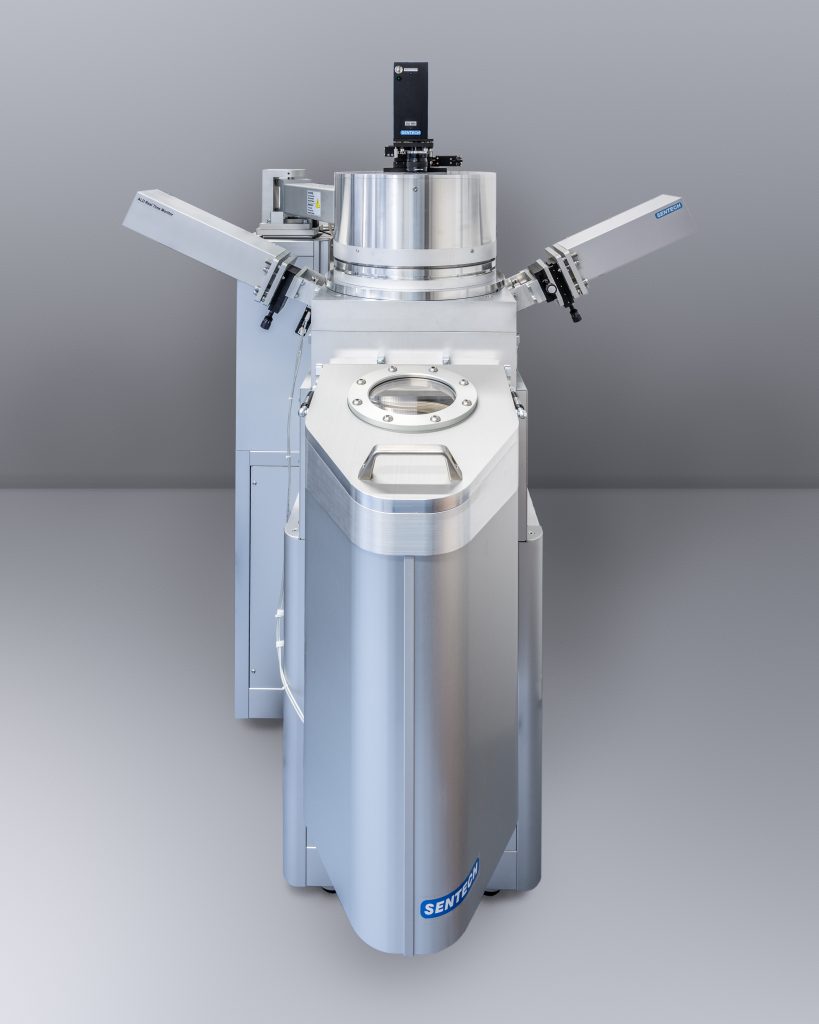
The SENTECH SE 500adv extends ellipsometric measurement capability by combining ellipsometry and reflectometry in a single system. This hybrid configuration eliminates thickness ambiguities and allows for accurate measurement of both ultra-thin and relatively thick transparent films—up to approximately 25 µm in total layer thickness.
For semiconductor researchers, this combination is particularly valuable when characterising complex layer stacks where films of different refractive indices and thicknesses coexist. The SE 500adv maintains the precision of a laser ellipsometer while adding the flexibility of a reflectometer, making it a comprehensive solution for materials characterisation, process monitoring, and optical design verification.
Why Laser Ellipsometry Matters to Semiconductor Research
As device dimensions continue to shrink, the demand for precise, non-destructive, and rapid measurement techniques continues to grow. Laser ellipsometry directly addresses these needs by providing:
- Unparalleled accuracy for ultra-thin layers.
- Material insight through simultaneous determination of thickness and refractive index.
- Scalability from R&D to production metrology.
- Compatibility with hybrid methods for complex structures.
By integrating high-precision instruments such as the SENTECH SE 400adv and SE 500adv into semiconductor workflows, researchers and engineers can ensure tighter process control, improved device performance, and faster innovation cycles.