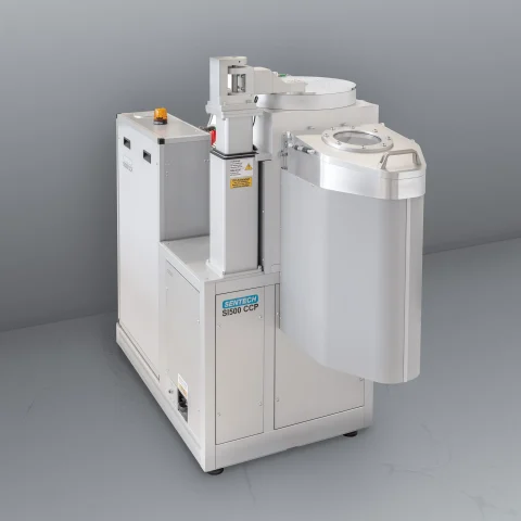
Reactive Ion Etching (RIE): The Foundation of Plasma Etching
What is RIE?
Reactive Ion Etching (RIE) combines chemical etching with physical ion bombardment to deliver precise pattern transfer. In RIE systems, a plasma is generated between two electrodes using a radio frequency (RF) power source. Reactive species chemically react with the substrate surface while positive ions accelerate toward it, physically sputtering atoms away.
When and Why Use RIE
RIE is ideal when moderate anisotropy and process control are required. It is widely used in:
- Photolithography pattern transfer for integrated circuits and MEMS devices.
- Dielectric layer etching, such as silicon dioxide or silicon nitride removal.
- Thin-film circuit patterning and surface cleaning prior to deposition steps.
Its balance of chemical and physical mechanisms makes RIE versatile and cost-effective for both research and production.
How RIE Works
The key to RIE’s success lies in the balance between ion energy and chemical reactivity. Adjusting gas composition, pressure, and RF power allows engineers to tune the process for optimal etch rate, selectivity, and sidewall profile, ensuring reliable, repeatable results across wafers.
Inductively Coupled Plasma Reactive Ion Etching (ICP-RIE): High-Density Plasma Precision
What is ICP-RIE?
Inductively Coupled Plasma Reactive Ion Etching (ICP-RIE) represents the next generation of plasma etching technology. It separates plasma generation and ion acceleration into two independently controlled systems:
- Inductively coupled RF coil – generates a high-density plasma.
- Bias power source – controls ion energy at the substrate.
This dual control enables deeper etching, improved anisotropy, and minimal substrate damage.
Why ICP-RIE is Essential for Advanced Semiconductor Devices
As semiconductor devices become smaller and more complex, ICP-RIE allows for precise etching of high-aspect-ratio structures with superior sidewall quality. It is indispensable in applications such as:
- Photonic crystal and waveguide etching
- MEMS and NEMS device patterning
- III–V compound semiconductor processing
How ICP-RIE Improves Process Control
ICP-RIE systems allow independent adjustment of plasma density and ion energy, giving process engineers fine control over etch uniformity, selectivity, and profile. This ensures repeatable, high-yield results, even in advanced node technologies.
Deep Reactive Ion Etching (DRIE): For High-Aspect-Ratio Structures
What is DRIE?
Deep Reactive Ion Etching (DRIE) is a specialised extension of ICP-RIE designed for deep, narrow trench and via etching in silicon and other materials. It alternates between etching and passivation steps, allowing vertical sidewalls and depths exceeding hundreds of micrometres.
Why DRIE Matters
DRIE is critical for MEMS fabrication, through-silicon vias (TSVs), and power semiconductor devices. It enables engineers to build three-dimensional structures essential for sensors, actuators, and packaging technologies.
How DRIE Works
DRIE typically uses the Bosch process, which alternates between a fluorine-based etch phase and a polymer deposition phase. This creates a near-vertical sidewall profile, essential for reliable device performance and integration density.
Cryogenic Etching: Ultra-Smooth and Damage-Free Surfaces
What is Cryogenic Plasma Etching?
Cryogenic etching operates at extremely low substrate temperatures (typically below −100°C). This temperature control reduces chemical reaction rates at unwanted surfaces, enabling smooth, damage-free sidewalls without polymer deposition.
When and Why to Use Cryogenic Etching
Cryogenic etching is ideal for optical and photonic applications, where surface smoothness is critical, and residue-free profiles are essential. It is commonly used in:
- Silicon photonics
- Nanoimprint lithography mold
- Quantum device fabrication
How It Enhances Etch Precision
By cooling the substrate, the process limits spontaneous chemical reactions, ensuring that etching only occurs where ion energy is directed — delivering ultra-clean results with high selectivity and minimal roughness.
Atomic Layer Etching (ALE): The Future of Plasma Processing
What is ALE?
Atomic Layer Etching (ALE) is a next-generation plasma etching technique that removes material at the atomic scale, one layer at a time. It uses self-limiting surface reactions to achieve unparalleled precision and uniformity.
Why ALE is Transformative
ALE is vital for sub-10 nm semiconductor nodes, quantum devices, and 2D material processing, where even nanometre-level deviations can affect device performance. It offers atomic-level control over etch rate, selectivity, and surface damage, critical for scaling beyond current lithography limits.
Why Plasma Etching is Essential in Semiconductor Device Applications
Plasma etching underpins nearly every modern semiconductor manufacturing process, from transistor gate definition to MEMS sensor release. Its ability to deliver nanometre-scale accuracy, material selectivity, and repeatability makes it indispensable for industries including:
- Integrated circuits (ICs) and logic devices
- Microelectromechanical systems (MEMS)
- Photonics and optoelectronics
- Power electronics and RF components
Without plasma etching, the miniaturisation, performance, and reliability of today’s electronic devices would be impossible.
SENTECH Plasma Etching Solutions
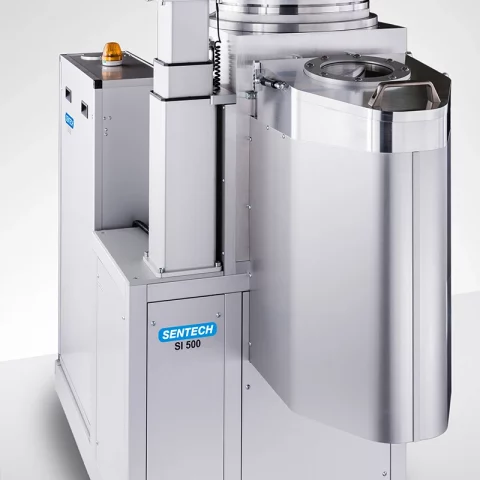
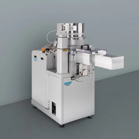
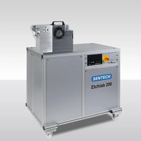
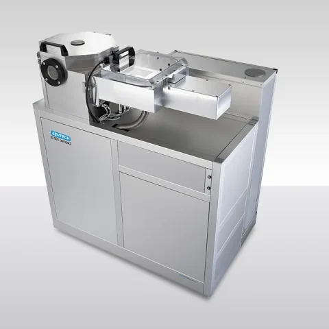
SENTECH Instruments is a global leader in plasma etching technology, providing advanced RIE, ICP-RIE, DRIE, Cryogenic, and ALE systems designed for both research and high-volume production environments.
SENTECH plasma etch systems deliver:
- Exceptional etch rate control and uniformity across wafers
- High selectivity for multi-material processing
- Superior sidewall profiles for deep and high-aspect-ratio features
- Modular, flexible configurations to suit diverse applications
With intuitive software control, low maintenance requirements, and reproducible performance, SENTECH plasma etching systems empower semiconductor engineers and researchers to push the boundaries of micro- and nanofabrication.
Precision, Control, and Innovation
SENTECH plasma etching technologies continue to evolve, enabling finer structures, better device performance, and higher manufacturing yields. SENTECH’s advanced plasma etching systems offer the precision, flexibility, and reliability required to meet the challenges of next-generation semiconductor device fabrication.

