What is Atomic Layer Etching?
Atomic Layer Etching (ALE) is an advanced, precision-driven nanofabrication technique designed to remove material at the atomic scale. Unlike traditional etching methods, which often struggle with accuracy, ALE enables manufacturers and researchers to achieve unparalleled control, uniformity, and selectivity in material processing. As devices become smaller, faster, and more complex, ALE has emerged as a key enabler for next-generation nanotechnologies and microtechnologies.
The technical implementation of Atomic Layer Etching (ALE) can vary depending on the material system and process configuration. However, all ALE methods share a fundamental characteristic: the etching process is divided into sequential steps consisting of (1) surface modification and (2) timely removal of the modified surface layer, separated by individual purge steps. This separation of surface activation and layer-removal enables atomic-level precision.
Both the modification and removal steps can be driven purely by chemical and thermal reactions, or they may be enhanced using plasma assistance. The advantage of plasma-assisted ALE lies in its ability to generate a high density of reactive radicals for surface modification, while providing a controllable ion bombardment to adjust the removal step to the specific material properties (e.g. binding energy).
By repeating these cycles, ALE achieves a precisely controlled etch depth determined by the number of cycles executed. Characteristic properties of ALE, such as surface smoothening, precise etch-depth control and excellent uniformity, arise from its inherently cyclic, layer-by-layer nature.
Industries and Applications of ALE in Nanotechnologies and Microtechnologies
The advancement of ALE plays a crucial role across several high-tech industries. In semiconductors, ALE enables the fabrication of ultra-thin transistors and high-performance integrated circuits. The microelectronics sector relies on ALE to create precise 3D structures for advanced memory and logic devices. In nanophotonics, ALE has been studied for fabricating nanoscale optical components, such as waveguides and resonators, with fine geometrical control and reduced surface roughness, improvements which can benefit communication and sensing applications. Beyond electronics, ALE is also important for the optimisation of high-frequency and high-power applications. ALE is already developed for GaN/AlGaN HEMT fabrication in photonics.
What are the Advantages of ALE Over Traditional Etching
ALE offers several distinct advantages compared to conventional etching processes. Its atomic-level precision ensures highly controlled removal of materials without damaging adjacent layers. This selectivity minimises defects and enhances device reliability. Unlike traditional methods, ALE achieves superior control over anisotropy and isotropy on the nanoscale, enabling the fabrication of advanced 3D device architectures.
Additionally, ALE provides better surface uniformity and smoothness, which is critical as device dimensions approach the sub-10 nm scale. This reduction in line-edge roughness leads to improved electrical performance and longer device lifespans. For industries demanding miniaturisation and high-performance nanostructures, ALE delivers a combination of precision, scalability, and reliability that conventional etching simply cannot match.
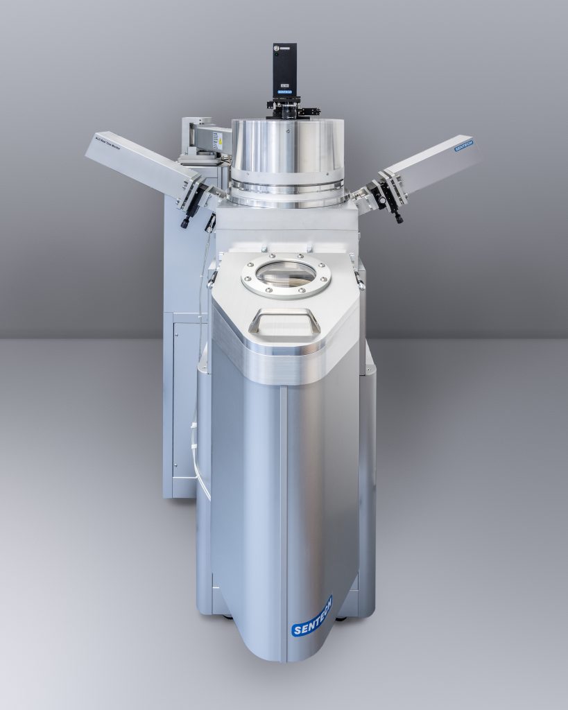
SENTECH offers the SI 500 ALE, an extension to the SI 500 ICP-RIE plasma etch system. The SI 500 ALE provides stable plasma at low operating pressure and low ICP power for low-damage etching with precise RF control. The key benefits are precise low-ion‐energy/ion bias control with the PTSA source, dynamic temperature and backside cooling control, in-situ process monitoring and efficient gas handling. If you have any questions or would like to speak to a member of our team, contact sales@sentech.de