The Paradox of Silicon Carbide – Exceptional Properties, Exceptional Difficulty
Silicon Carbide (SiC) has become a cornerstone material for advanced power electronics, high-frequency devices, and harsh-environment sensors. Its wide bandgap and thermal conductivity provide device designers with the ability to achieve higher voltage blocking, faster switching, and improved efficiency compared to silicon.
However, these same intrinsic properties that make SiC technologically attractive also make it one of the most difficult materials to process in semiconductor manufacturing. Its chemical inertness, strong covalent bonding, and high hardness demand extreme precision in every process step, from substrate preparation to etching, dielectric deposition, and thin-film characterisation. Understanding the fundamental challenges of SiC processing is essential for developing reliable, reproducible, and scalable device fabrication technologies.
The Challenges of SiC Etching
Hardness and Chemical Resistance
SiC’s strong Si–C bonds make it remarkably resistant to chemical attack. As a result, purely chemical plasma etching is inefficient, and physical ion bombardment must contribute significantly to material removal. This combination leads to slow etch rates and a high risk of plasma-induced surface damage.
Reactive ion etching (RIE) of SiC typically requires high-density plasmas containing fluorine or chlorine radicals (SF₆, Cl₂, BCl₃) with energetic ion assistance to achieve practical etch rates. Maintaining process control in such high-energy environments is difficult. Excessive ion energy introduces lattice defects and roughness, while insufficient ion assistance results in poor anisotropy and residue formation.
Anisotropy and Mask Selectivity
Etching high-aspect-ratio SiC features requires a balance between chemical and physical etching mechanisms. Too much physical sputtering causes mask erosion and sidewall damage. Too little leads to isotropic profiles. Achieving vertical sidewalls with minimal “trenching” is a persistent challenge, especially for deep structures like power device trenches or MEMS cavities.
Mask materials such as SiO₂ or Si₃N₄ are typically used due to their hardness and plasma resistance, but the etch selectivity between SiC and these materials is often low. Poor selectivity increases process time, cost, and the likelihood of micro-masking from redeposited material.
Surface Damage and Contamination
The high-energy ion bombardment necessary to etch SiC can produce lattice disorder, amorphisation, or local charging, which in turn affects the electrical characteristics of subsequent device layers. These damaged regions can act as traps or leakage paths, reducing channel mobility in MOSFETs and altering threshold voltages. Managing ion energy, plasma uniformity, and bias power is critical to minimising such effects.
Deposition Challenges for Dielectric and Passivation Layers on SiC
Interface Quality
Device performance and reliability in SiC electronics are largely determined by the quality of the dielectric interface. For example, the SiC/SiO₂ interface density of states (Dit) is several orders of magnitude higher than that of Si/SiO₂, resulting in lower effective channel mobility in SiC MOSFETs. Plasma-induced damage or contamination during processing can exacerbate these interface defects.
Temperature and Stress Constraints
High-quality SiO₂ and Si₃N₄ films require sufficient energy for complete precursor dissociation and densification, typically achieved at temperatures above 400 °C in conventional PECVD. However, many SiC devices incorporate metallisation, dopant implants, or temperature-sensitive structures that limit allowable process temperatures. The result is a need for low-temperature plasma deposition methods that can still deliver dense, low-stress films.
Stress control is particularly critical for SiC due to its stiffness and low thermal expansion coefficient. Even moderate intrinsic film stress can lead to cracking or delamination, especially on patterned or high-aspect-ratio surfaces.
Step Coverage and Uniformity
Deep trenches and textured SiC surfaces further complicate dielectric deposition. Achieving conformal coatings in these geometries requires high-density plasmas and precise control of ion directionality and radical flux. Traditional PECVD often produces voids or poor step coverage in such structures, necessitating more advanced techniques such as inductively coupled plasma-enhanced CVD (ICPECVD) or plasma-enhanced atomic layer deposition (PEALD).
Metrology and Process Control Challenges
SiC device fabrication pushes the limits of thin-film metrology. The optical contrast between SiC and common dielectrics is weak, and many SiC structures involve multilayer stacks with nanometer-scale variations. Non-destructive techniques capable of resolving these differences are essential.
Spectroscopic ellipsometry is particularly suited to this task, as it measures both amplitude and phase changes in reflected light, allowing extraction of film thickness and optical constants (n, k) with sub-nanometer precision. However, ellipsometric modelling of SiC is complex due to its anisotropy and strong phonon absorption in the infrared region. Accurate measurement, therefore, depends on,
- Wide spectral coverage (UV–NIR–IR) to distinguish overlapped optical responses
- Precise polarisation control to handle anisotropic films
- Automated data analysis and mapping for wafer-scale uniformity studies
Integrating such measurement tools in-line or at-line allows real-time feedback between etch, deposition, and characterisation steps, an increasingly important factor in process stability and yield improvement.
Overcoming SiC Processing Barriers with Advanced Plasma Systems
Addressing SiC’s etching and deposition difficulties requires plasma sources capable of high ion density, independent energy control, and fine gas-chemistry management. Modern systems such as Inductively Coupled Plasma Reactive Ion Etching (ICP-RIE) and Inductively Coupled Plasma-Enhanced CVD (ICPECVD) provide the flexibility to tune both ion flux and bias power independently, enabling process engineers to balance etch rate, anisotropy, and surface damage.
For atomic-scale control, PEALD extends these principles further, using self-limiting surface reactions to achieve uniform film growth at low temperatures with excellent conformality. This approach is especially valuable for gate oxides and interface engineering in SiC MOSFETs and high-frequency devices.
In all cases, the combination of stable plasma generation, in-situ diagnostics, and stress-tunable process control represents the key technological pathway to reproducible SiC process integration.
SENTECH’s plasma process platforms, the SI 500 ICP-RIE, SI 500 D ICPECVD, and SI PEALD systems, are examples of tools developed around these principles. Each employs high-density plasma sources with independent bias control and in-situ monitoring to achieve the precision, repeatability, and low-damage processing necessary for advanced SiC fabrication.
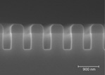
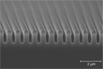
SEM image of SiC trench 1 μm deep after 90 s etch time, using a SiO2 hard mask, showing smooth, vertical side walls with no trenching
Characterising Layers with Optical Precision
Equally essential is the ability to verify the results of each process step without destructive testing. Spectroscopic ellipsometry, reflectometry, and in-situ optical monitoring allow for continuous tracking of layer thickness, refractive index, and uniformity.
Systems such as SENTECH’s SENresearch 4.0, SENDIRA, and SENDURO accuva10 exemplify the role of precision metrology in SiC process development, offering broad spectral coverage, full Mueller-matrix analysis for complex films, and automated wafer handling for statistical process control. This combination of high-density plasma processing and optical metrology establishes the feedback loop necessary for consistent, high-yield SiC manufacturing.
A Unified Approach to SiC Fabrication
Processing SiC demands a departure from traditional silicon fabrication paradigms. Its hardness, chemical inertness, and interface sensitivity require plasma sources capable of delivering controlled high-energy ions, deposition techniques that ensure low-temperature film densification and stress management, and metrology systems precise enough to characterise nanometer-scale variations.
The key elements to overcoming these challenges are:
- High-density, independently controlled plasma environments for etching and deposition
- Low-damage processing and stress-optimised dielectric growth
- Conformal coating techniques such as ICPECVD and PEALD
- Non-destructive, high-resolution metrology for continuous process feedback
By integrating these capabilities within a single process and characterisation framework, SENTECH provides a comprehensive technology platform for SiC fabrication, combining precision plasma process systems with advanced optical metrology. Together, these tools enable engineers to reliably control every stage of SiC wafer processing, paving the way for the next generation of high-performance semiconductor devices. To request our latest SiC SENTECH Solutions brochure, contact us