Shanghai, 31.05.2018
SENTECH Plasma Process Technology Seminar in Shanghai
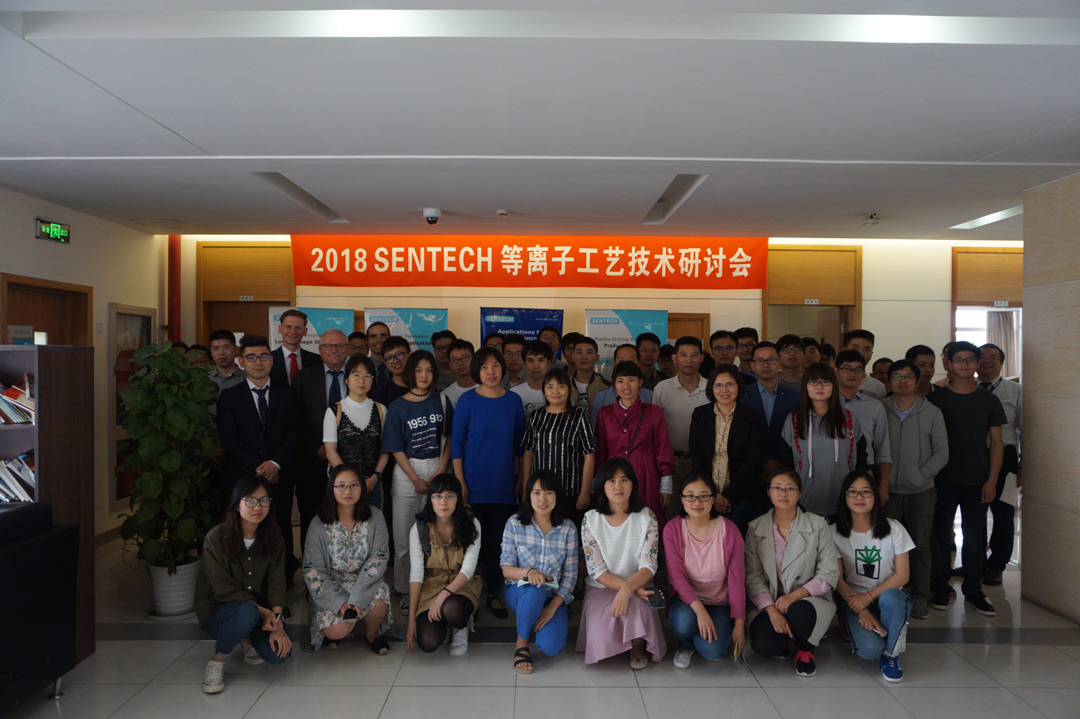
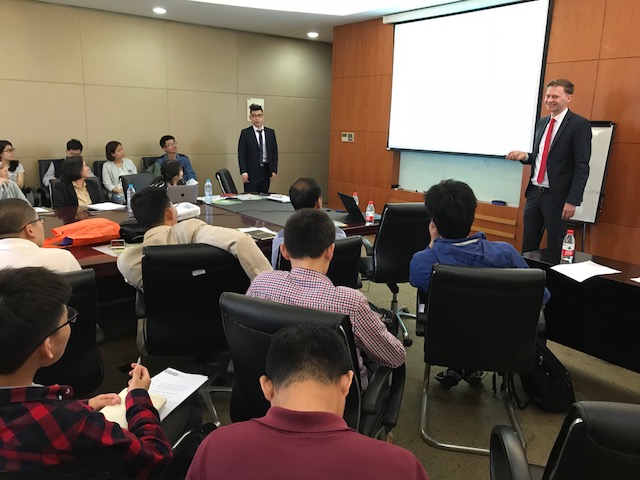
SENTECH, a specialist in plasma etching, plasma deposition, atomic layer deposition and insitu measurement methods, presented the newest results in etching silicon and III-V compounds, in depositing dielectric films for device passivation by ICPECVD, in ALD for optical and high frequency device applications as well as in advanced automation. Applications and outstanding properties of etched and deposited films achieved by SENTECH plasma tools were emphasized in the presentations. Prof. Chen gave an interesting insight into the work of the AEMD and the capability of the center in terms of device manufacturing. SENTECH latest results for advanced automation for plasma processing were presented especially for production.
The lively discussion during and after each presentation showed the great interest in the presented data and results. SENTECH China Sales Office and SENTECH Germany organized the Plasma Process Technology Seminar in the Center of Advanced Electronic Material and Devices of Shanghai Jiao Tong University on May 31, 2018. More than 60 participants from local universities, institutes, and companies took part in this seminar. We thank all participants for their interest and their engagement in the discussion. Especially, we would like to thank Prof. Chen, the head of the AEMD, for her hospitality and support for the SENTECH Plasma Process Technology Seminar in Shanghai.