

Plasma Process Technology
Thin Film Metrology
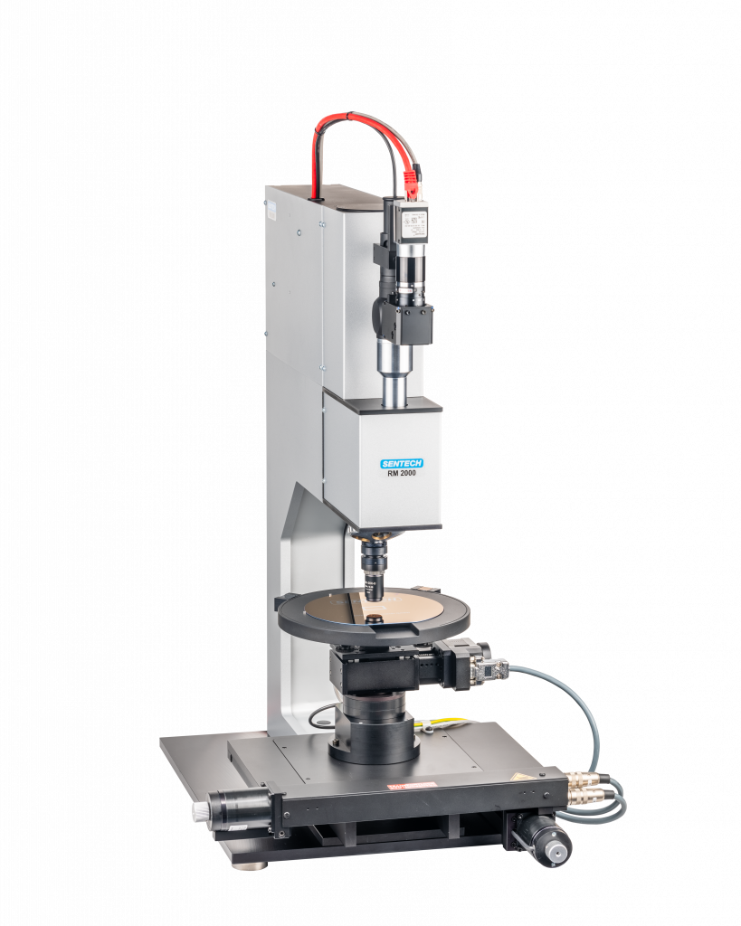
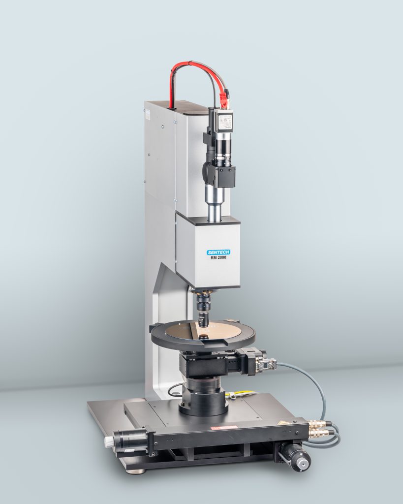
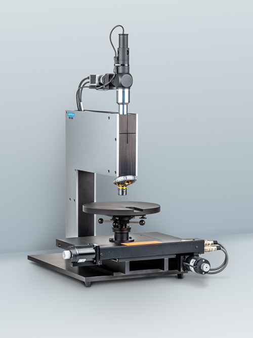
The spectroscopic reflectometry using the RM 1000/2000 features UV to NIR spectral range from 200 nm – 1000 nm. The optical layout is optimised for light throughput for reliable measurements of n and k even on rough or curved surfaces and with precise height and tilt adjustment.


SENTECH spectroscopic reflectometers feature the most accurate single beam reflectance measurements by height and tilt adjustment of a sample and by high light conductance of optical layout, allowing repeatable measurements of n and k, measurements on rough surfaces, as well as thickness measurements of very thin films.
RM 1000 | 410 nm - 1000 nm
RM 2000 | 200 nm - 1000 nm
The spectroscopic reflectometers RM 1000 and RM 2000 can optionally be equipped with an x‑y mapping stage and mapping software and an objective lens for small spot sizes.
The RM 1000 and RM 2000 spectroscopic reflectometers measure the reflectance of flat or curved samples with smooth or rough surfaces. The thickness, extinction coefficient, and refractive index of single films or layer stacks are calculated using the SENTECH FTPadv Expert software. Single films between 2 nm and 50 µm thickness (RM 2000) or 100 µm (RM 1000), respectively, layer stacks, and substrates can be analysed in the UV‑VIS‑NIR spectral range.
Thickness map of photoresist / Si (substrate) with step size of 50 µm and 25 µm
Reflection measurement
on rough surfaces
X-y mapping stage
The SENTECH RM 1000 and RM 2000 represent our high-end reflectometers. The tabletop device comprises the highly stabilised light source, the reflection optics with auto-colliation telescope and microscope, a camera, the height and tilt adjustable sample platform, the spectral photometer, and the power supply. It can be optionally equipped with an x‑y mapping stage and mapping software, and an objective lens for a second spot size.
Besides film thickness and optical constants, the composition of films (e.g. of AlGaN on GaN, SiGe on Si), AR coating (e.g. on textured silicon solar cells, UV-sensitive GaN devices), and coatings on small medical stents can be measured by our reflectometers. These reflectometers support applications in microelectronics, microsystems technology, optoelectronics, glass coatings, flat panel technology, life science, biotechnology, and others.
The comprehensive, recipe-oriented SENTECH FTPadv EXPERT software for our reflectometers RM 1000/2000 includes measurement set-up, data acquisition, modelling, fitting, and reporting. An extensive database of predefined customer-proven and ready-to-use applications is already built in. The AutoModel option allows for the automatic selection of sample models from a spectra library. Based on SENTECH expertise in spectroscopic ellipsometry, a large materials library and the variety of dispersion models allow the analysis of nearly all materials and films by our spectroscopic reflectometers. The data library can easily be updated with new optical data by the operator. SENTECH supports its customers with the measurement of new materials with unknown optical properties by spectroscopic ellipsometry.
Material database including:
SENTECH has a large team of application experts for both plasma process technology and thin film metrology. At our campus are two laboratories which are used to process and characterise customer samples, for system demonstrations and customer training. SENTECH offers application support for the lifecycle of your system. Learn more about our application support or contact the team.
Yes, SENTECH has two application labs in-house. You can contact our application team, who will share with you all the details and provide a sample analysis form for you to complete. Click here for further information and contact details.
Yes, SENTECH has a large network of technical service experts who offer in-country support for both plasma process technology and thin film metrology systems. Remote or on-site support is possible depending on your requirements. Click here to find out more or to contact the team.