


SENTECH Instruments develops, manufactures, and sells worldwide advanced quality instrumentation for Plasma Etching, PECVD, Atomic Layer Deposition, Thin Film Measurement (Spectroscopic Ellipsometry, Spectroscopic Reflectometry and Laser Ellipsometer) and Photovoltaics.
What's New?
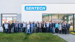
This year’s SENTECH Plasma Process Technology Seminar on 25 April 2024, in Berlin-Adlershof, was once again a great forum for ideas and networking. You can read a summary on all the news from the event here.
→read more
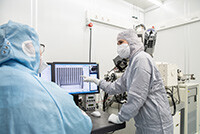
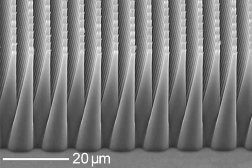
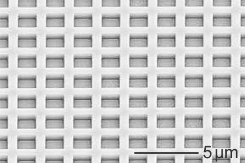
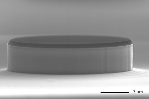
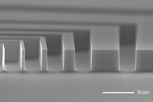
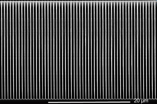
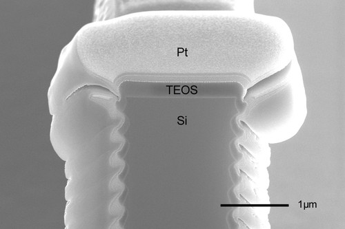
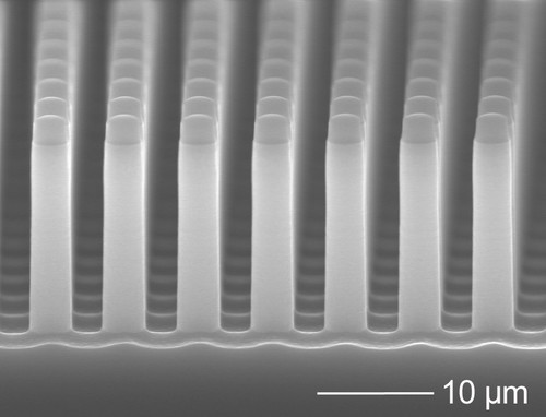
Find out more about how a SENTECH ICP-RIE Plasma System was used by researchers from the Fraunhofer Institute for Applied Optics and Precision Mechanics IOF and the Institute of Applied Physics IAP at the Friedrich Schiller University to develop diamond microstructures for precise measurement in the extremely remote infrared range →read more
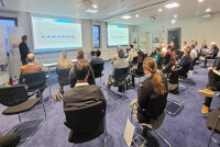
The SENTECH Thin Film Metrology Seminar and Workshop took place on 29 – 30 November 2023 in Berlin-Adlershof. Read the full article to find out more about the seminar and all of the topics from this year's event. →read more
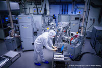
Find out about the collaboration between SENTECH and “Research Laboratory Microelectronics Bochum for 2D Electronic Systems” (ForLab PICT2DES) at Ruhr-Universität Bochum (RUB) project to learn more about the atomic layer deposition (ALD) for 2D materials. Request your copy of the case study here. →read more
ICP-RIE Plasma Etching:
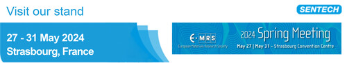
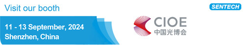
Upcoming Events:


SENTECH
Instruments GmbH
Schwarzschildstr. 2
12489 Berlin
Germany
Phone: +49 (0)30 63 92 55 20
Fax: +49 (0)30 63 92 55 22
Email: info@sentech.de