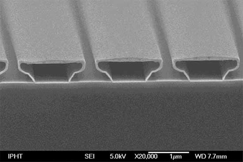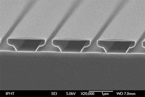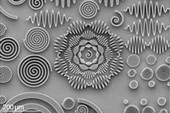


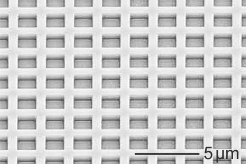
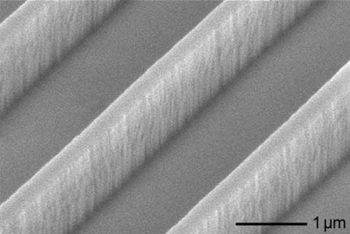
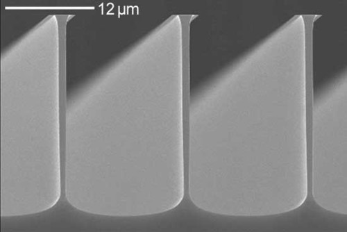
- RIE etcher
- ICP-RIE etcher
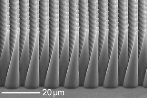
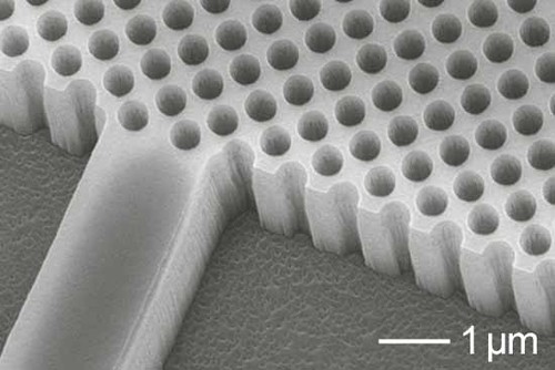
- Deep RIE etcher

- PECVD deposition
- ICPECVD system
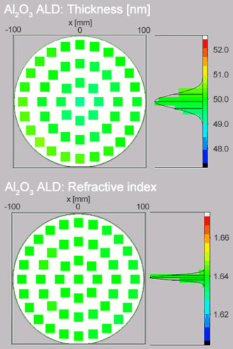
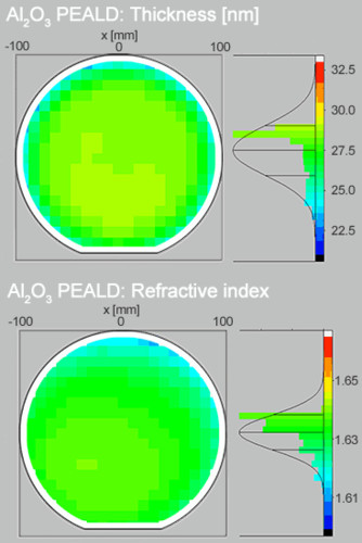
- Atomic layer deposition
- Thermal ALD
- PEALD
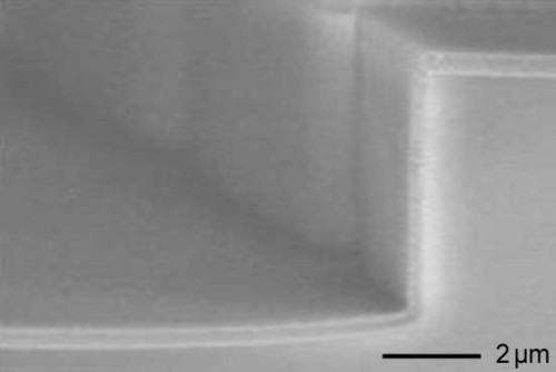
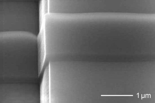
RIE Etching
| Characteristics: | low damage, high rate, anisotropic etching, high density, low ion energy distribution |
| Materials: | III-V compound semiconductors (GaAs, InP, GaN, InSb), silicon, silicon compounds (SiC, SiGe), dielectrics, quartz, glass, metals, polymers, sapphire |
| Applications: | nanostructuring, MEMS, quantum devices, lasers, transistors, high frequency devices, microoptics |
PECVD Deposition
| Characteristics: | low temperature, low damage deposition, low stress, low interface state density, low pin hole density, high breakdown voltage |
| Materials: | dielectrics (SiO2, SiNx, SiOxNy), undoped and doped amorphous silicon (aSi:H), SiC |
| Applications: | passivation, barriers, membranes, masks, isolation, optical coatings |


Atomic Layer Deposition
| Characteristics: | conformal, pinhole- and particle-free, nano-scale controlled, low temperature deposition |
| Materials: | oxides, nitrides, metals |
| Applications: | passivation, 3D deposition, OLEDs, barriers, adhesion layers, optical coatings, high k applications, biomedical applications |