MDPinline
Inline Full Wafer Map in Less Than One Second

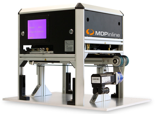
The MDPinline is Production integrated high speed wafer mapping of carrier lifetime. Single wafer topograms in less than one second a wafer.
The MDPinline is a compact high speed production integrated mapping tool for quantitative measurements of carrier lifetime. Topograms are measured ‘on the fly’ in less than a second a wafer while the wafers are moved underneath the instrument by the conveyor as installed in the factory.
The MDPinline itself uses no mechanically moving parts making it extremely reliable also under continuous operation. The availability of a full topogram for each individual wafer offers new ways to increase the cost effectiveness and efficiency of production lines which were so far completely out of scope. For example, an automated statistical evaluation of 10.000 wafer topograms, which are obtained within less than three hours, reveal surprisingly fine details of the performance of crystal growth furnaces as well as material quality. Processing steps such as diffusion and passivation may be ramped up and optimised within so far impossible timescales at highest performance, due to real time quality and homogeneity investigation. In the running production, any failure of a processing step may be detected immediately. On the other hand, if wafers are sold to a customer, higher prices are achieved, if each wafer exhibits a guaranteed performance leading to a return of investment for the MDPinline within less than a year.
Advantages
- Full electrical wafer characterisation at speeds up to one wafer in less than a second. Measured parameters: Carrier lifetime (full topogram), resistivity (two line scans).
- So far not seen efficiency of process control, yield and process improvement allow for an extremely fast upramping of new fabs or processes, since statistical information from thousands of wafers are obtained in a very short period of time.
- Suitable for measurement of material quality of outgoing or incoming wafers as well as identification of crystallisation problems at wafer level for instance in PV industry. Well suited for diffusion process integrity control, passivation efficiency and homogeneity control.
Documents To get more information, please contact SENTECH GmbH or visit Freiberg Instruments.
Documents To get more information, please click here or visit Freiberg Instruments.


