What Is Plasma Deposition and Why Does It Matter in Modern Semiconductor Fabrication?
Plasma deposition has been around since the late 18th century (1) when the first electric arcs were observed and studied. In the early 19th century, W.R. Grove discovered sputtering (2) , where a cathode in a vacuum discharge tube scraped and deposited material on the tube walls. The term “Plasma” was introduced later on in 1928 by Irving Langmuir (3). By the 1950s, research into reactive sputtering began, a precursor to modern coating technologies (4) , and as we entered the 1960s, coatings began to be considered for large-scale commercial use (5). Today, plasma deposition has become one of the most critical enabling technologies in contemporary semiconductor fabrication, powering advances in microelectronics, nanotechnology, photonics, and high-performance optical coatings.
As devices become smaller, thinner, and more functionally complex, manufacturers must create ultra-uniform films on wafers and substrates that often have challenging chemistries, high aspect-ratio structures, or strict thermal parameters. The question of how to deposit films with atomic-level precision, excellent step coverage, and strong material compatibility has driven increasing interest in plasma-enhanced processes. Among these, Plasma-Enhanced Chemical Vapour Deposition (PECVD), Inductively Coupled PECVD (ICPECVD), Atomic layer deposition (ALD) and Plasma-Enhanced Atomic Layer Deposition (PEALD) stand out as core methods for producing high-quality thin films used in advanced semiconductor and optical applications.
How Does PECVD Work and When Is It the Best Deposition Method?
PECVD is widely used because it enables low-temperature deposition of dielectric and semiconductor thin films such as silicon nitride, silicon oxide, amorphous silicon, and various passivation layers. By generating plasma from precursor gases, PECVD activates chemical reactions at temperatures significantly lower than those required by traditional, thermally activated CVD. This makes it ideal for temperature-sensitive substrates, including those used in photovoltaics, MEMS, sensors, and integrated photonics. High-density PECVD, also known as ICPECVD, is an advanced PECVD technique, where an extra high-density plasma is reacted by means of inductive coupling
Under What Conditions Does PECVD Provide an Advantage?
PECVD excels when manufacturers need high deposition rates, good uniformity across large wafers, and reliable film properties at moderate cost. It is particularly well-suited for optical coatings in integrated photonic devices, where controlled refractive indices and low stress are crucial. In micro- and nanotechnologies, PECVD is often the method of choice for passivation, antireflection coatings, and insulating layers in microelectronics.
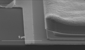
When processing wide-bandgap materials such as silicon carbide, PECVD provides an effective route to depositing dielectric layers without exposing the substrate to temperatures that could affect dopant profiles or thermal stability. However, PECVD does have limitations. When extreme conformality is required, such as when coating deep trenches or ultra-narrow vias, PECVD may struggle to achieve optimal levels of uniform step coverage due to its line-of-sight transport mechanisms. This has driven increasing interest in plasma processes with higher density and more directional control.
What Makes ICPECVD Different and Where Does It Solve Deposition Challenges?
Inductively Coupled PECVD, ICPECVD or high-density PECVD, evolved to address situations where conventional PECVD cannot deliver sufficient film quality or conformality. By using an inductively coupled plasma source, such as the SENTECH PTSA source, ICPECVD generates a much higher plasma density, enabling greater degrees of ion control and improved energy delivery to the substrate surface. This enhanced plasma environment encourages more complete precursor dissociation and stronger surface activation, leading to higher-quality films with better mechanical and electrical properties at lower deposition temperatures (<130 °C).
Where is ICPECVD Most Beneficial?
It becomes the preferred technique for dense, low-defect films in advanced semiconductor nodes, deep-etch MEMS structures, or high-performance optical stacks. In nanotechnology, ICPECVD is often chosen when deposition must penetrate complex topographies or when exceptionally low film stress is required to avoid wafer bowing or membrane distortion. For applications involving silicon carbide, ICPECVD offers good adhesion and dielectric performance, especially when producing high-k dielectrics or protective barrier layers.
In contrast to PECVD, using ICPECVD alongside carefully optimised process parameters such as plasma power, precursor flow, and low substrate temperatures, high-quality films can still be achieved without sacrificing high deposition rates. It’s possible to maintain excellent film uniformity, density, and functional properties while maintaining throughput. This approach allows for production-scale processing without sacrificing the performance or reliability of devices.
Another advantage emerges where process flexibility is essential. The independently controlled ion energy and plasma density allow ICPECVD systems to tune film characteristics, such as refractive index, density, and compressive or tensile stress, with greater precision. This makes it an excellent option for process engineers developing next-generation devices with distinct electrical or optical specifications.
How Does ALD Achieve Atomic-Scale Control and When Should It Be Used?
Atomic Layer Deposition is fundamentally different from PECVD and ICPECVD due to its reliance on self-limiting surface reactions. Rather than depositing material continuously, ALD introduces precursor gases sequentially, allowing each precursor cycle to form a single atomic layer. This results in high levels of conformality, exceptional film uniformity, and thickness control down to the angstrom level.
When is ALD the Best Option for Semiconductor Manufacturing?
ALD is ideal when absolute precision matters, especially in advanced transistor gate dielectrics, barrier layers, and ultrathin high-k materials. In nanotechnology, ALD enables coating of 3D nanostructures and high-aspect-ratio features that no other deposition method can reliably cover. For silicon carbide devices, often used in high-temperature, high-voltage, or high-frequency electronics, ALD produces high-integrity dielectric layers that withstand extreme operating conditions while maintaining low defect densities.
Where Does Plasma-Enhanced ALD (PEALD) Become Critical?
PEALD incorporates plasma activation by radical species, not available in purely thermal processing, and enhances surface reactions, allowing the use of a broad range of precursor materials and deposition at temperatures as low as room temperature, which is invaluable for compound semiconductors, optical polymers, and delicate nanostructures that cannot tolerate high heat. PEALD also improves film density and stoichiometry, making it suitable for demanding 2D materials, optical coatings or moisture-barrier layers.

How Do PECVD, ICPECVD, and ALD Compare in Terms of Performance and Applications?
Selecting the right deposition method depends on the balance of film quality, throughput, conformality, and temperature constraints. PECVD delivers an excellent cost-to-performance ratio for mainstream applications and remains a workhorse in fabs and research labs. ICPECVD offers a step change in film density and process control, making it well-suited to advanced optical stacks, MEMS, SiC devices, and microelectronics requiring durable and low-stress coatings. ALD and PEALD provide the ultimate solution for atomic-level precision, especially when working with nanoscale features or when ultra-uniform films are essential for device reliability.
Understanding when and where each technology should be applied is now a central question in process development for modern semiconductor fabrication. As device geometries shrink and material systems become increasingly complex, the ability to select the appropriate deposition method is crucial for ensuring optimal performance, reliability, and scalability.
What Does the SENTECH Range of Deposition Tools Offer?
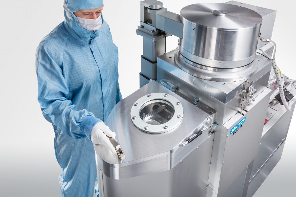
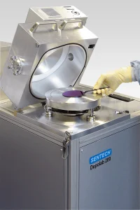
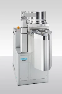
SENTECH provides a flexible, modular and versatile portfolio of plasma deposition systems designed to address a wide spectrum of semiconductor, optical, and nanotechnology applications for both research and production laboratories. The SENTECH Depolab 200 PECVD open lid system delivers reliable PECVD thin films with excellent uniformity and stress control, well-suited to hard masks, photonics, MEMS, microelectronics, and protective coatings. The SENTECH SI 500 D ICPECVD system provides high-density plasma environments that enable superior film properties, improved conformality, and precise stress control, making them ideal for advanced technologies, including silicon carbide processing and high-performance optical stacks. For applications demanding atomic-scale precision and maximum flexibility at low footprint, the hybrid SIPAR ICP deposition system combines ICPECVD and PEALD in one reactor. The SENTECH SI PEALD has the option to be fitted with either the PTSA ICP or True Remote CCP source, which provides exceptional control over film thickness and material quality, supporting next-generation quantum-computing, 2D-devices, micro- and nanodevices where uniformity and conformality are paramount. Real-time process monitoring and End Point Detection (EPD) of ALD and PEALD processes is enabled by the SENTECH AL Real Time Monitor for in-situ process control with superior time and thickness resolution.
For over thirty years, SENTECH systems, developed and manufactured in Berlin, Germany, have given researchers and manufacturers in the semiconductor industry the flexibility to choose the most effective deposition approach for specific material, structural, and performance requirements. When you choose a SENTECH system, you receive application support for the lifecycle of your tool, ensuring that modern thin-film challenges can be met with confidence.
References
1. Anders, André. “Tracking down the origin of arc plasma science I. Early pulsed and oscillating discharges.” IEEE Transactions on Plasma Science, 2003
2. Foundations of Vacuum Coating Technology, by Donald M. Mattox (SVC).
3. Cambridge University Press, Introduction to Theoretical and Applied Plasma Chemistry
4. Greene, J. E. “Tracing the recorded history of thin-film sputter deposition”, J. Vac. Sci. Technol. A, 2017
5. A Concise History of Vacuum Coating Technology (STERC).