Corporate News
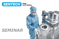
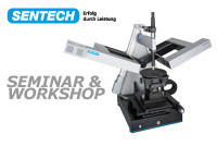
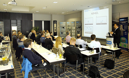
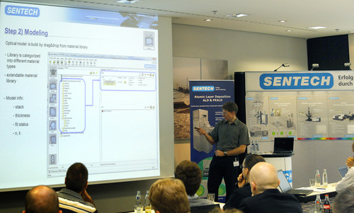
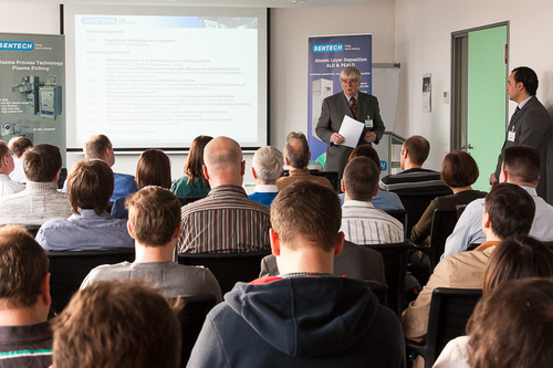
SENTECH offers an application oriented seminar “Plasma-Process-Technology” on April 7, 2022 at SENTECH in Berlin-Adlershof. Applications for low damage etching and deposition will be presented in sensors, quantum and III-V-devices. →read more
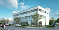
SENTECH Instruments GmbH celebrates the topping-out ceremony for a new building. The new facilities are built to increase production warehouse and administration area. SENTECH was celebrating the ceremony in the Science and Technology Park Berlin Adlershof on July 17, 2019. →read more
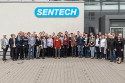
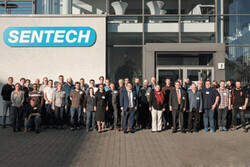
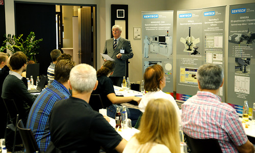
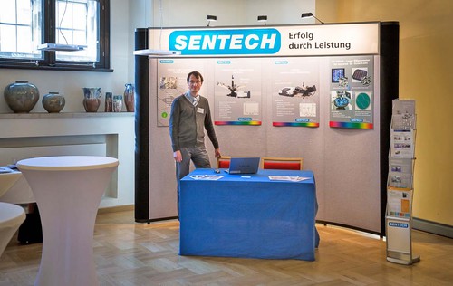
In good tradition SENTECH GmbH, Krailling hosted the SENTECH Seminar on Plasma Process Technology. The event took place on March 28, 2019. The seminar has become a meeting place for long-time users of SENTECH plasma tools and new customers.
40 experts of plasma process technology shared their experience in etching and coating with plasma systems and ALD systems. →read more
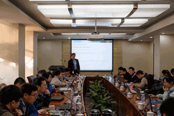
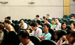
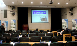
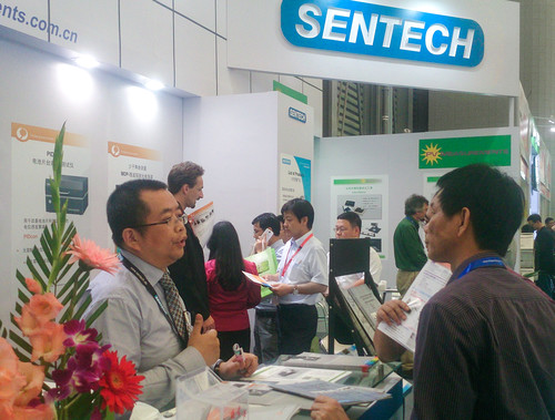
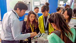
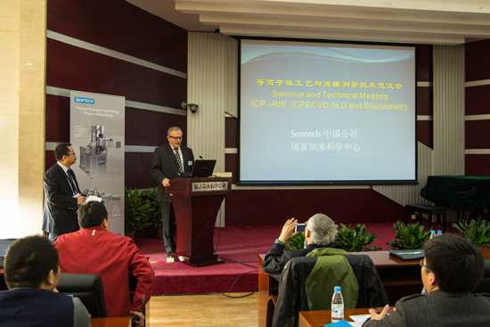
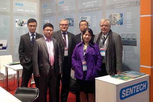
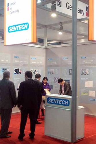
A SENTECH workshop on Ellipsometry took place in January 9-11, 2019 in Beijing, China. There is an large interest of Chinese scientists and users in SENTECH innovative thin film measurement tools. That’s why SENTECH is organizing application-oriented workshops and seminars in China frequently. This is to update already existing users as well as prospective customers on new metrology applications and their possibilities of use. →read more
On November 6th, 2018 SENTECH organized the seminar "Ellipsometry and Reflectometry for Quality Control of Thin Films" in Berlin-Adlershof. Professional external speakers as well as SENTECH experts gave presentations on possible applications of optical measurement techniques of ellipsometry and reflectometry.. →read more
SENTECH veranstaltet am 28. März 2019 ein anwendungsorientiertes Seminar über das Thema „Plasma Prozess Technologie“ in den Räumen von SENTECH Instruments in Berlin Adlershof. Aktuelle Themen sind das schädigungsarme Ätzen und Beschichten in der Prozessierung von Bauelementen, 3d-konforme Abscheidung dünnster Schichten und industrielle Anwendungen in der Plasma-Prozess-Technologie. →read more
SENTECH veranstaltet ein anwendungsorientiertes Seminar zum Thema „Ellipsometrie und Reflektometrie zur Qualitätskontrolle dünner Schichten“ in Berlin-Adlershof. Wir freuen uns, dass wir auch dieses Jahr wieder kompetente Referenten gewinnen konnten, die Ihnen an ausgewählten Beispielen die Anwendungsmöglichkeiten der optischen Messtechniken Ellipsometrie und Reflektometrie von SENTECH erläutern werden. →weiter
Previous News:
SENperc PV wins Innovation Award 2016
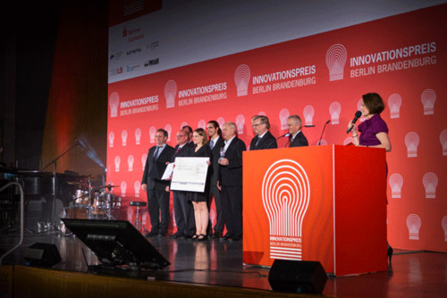
SENTECH is winner of the Innovation Award 2016 Berlin Brandenburg. The SENperc PV was honored as one of the five most innovative products of 2016. The SENperc PV is used for quality control for PERC cell back side manufacturing in the photovoltaic sector. Within the ceremony on December 2, 2016 at the Henry-Ford-Building of the TU Berlin the price was handed to the SENTECH employees.
The Innovation Award 2016 is an annual event targeting to promote innovate products which are generating the jobs of the future for the region of and around Berlin. SENTECH SENperc PV is a system for quality control in photovoltaics. It guarantees the efficiency and quality of PERC solar cell manufacturing. A video, produced by the Innovation Award Team, is showing the background as well as the way of functioning of the SENperc PV: Video-Stream.
“Despite the fact we have been sure, that our SENperc PV is a very innovative system which perfectly meets the demand of the photovoltaic sector, we have been very anxious about the result of the ceremony. The 10.000€ price money will be invested in further innovation processes. Of course also our employees will benefit from this too.“ says Dr. Albrecht Krüger, CEO of SENTECH Instruments GmbH.
SENTECH is more than happy about SENperc PV convinced the jury of the Innovation Award 2016 Berlin Brandenburg. Prospectively we will work hard on our innovation power to be part of the Berlin/Brandenburg economic engine further on. For more information on SENTECH photovoltaic measurement tools contact us here!
(Pictures by T. Ecke/Innovationspreis)SENperc PV awarded at SNEC Show 2016
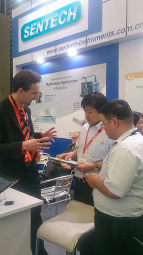
SENTECH presented the new, innovative SENperc PV – a metrology tool for quality control in PERC solar cell manufacturing. Al2O3/SiNx layer stacks and single films for passivation of PERC solar cells are measured. The SENperc PV was introduced for the first time in China. It was awarded at the on-site session of the SNEC Show as one of the “Top 10 Highlights” as innovative product launch in 2016. Dr Gruska, Marketing Manager at SENTECH introduced the new quality control tool.
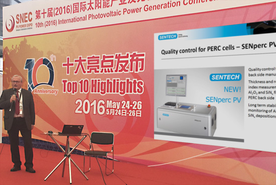
The SENperc PV measures thickness and refractive index of single Al2O3 and SiNx films and Al2O3/SiNx layer stacks on the back side of PERC solar cells. Easy recipe based operation and statistical process control make the SENperc PV the ideal tool for quality control of PERC passivation layers. Direct and long-term feedback to the operator for immediate intervention drew attention to the new SENTECH tool at SNEC PV Power Expo.
Further, SENTECH promoted the widely used and well-known SE 400adv PV and SE 800 PV. Over the last years the SE 400adv PV became the worldwide standard for quality control of antireflective coatings on the front site of Si solar cells. The SE 800 PV is the ideal tool for R&D of multilayer stacks for passivation and AR coating of Si solar cells.
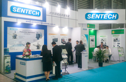
The SNEC PV Power Expo is important to SENTECH as one of the world leading photovoltaic exhibitions. This annual event takes place in Shanghai, China and attracts several thousands of visitors yearly. At 2150,000 sqm more than 1500 exhibitors presented innovative solutions and new products for the production of clean and sustainable energy.
SENTECH gained very good response for its powerful quality control tools for present and future challenges in silicon photovoltaics. SENTECH wants to thank the numerous customers for visiting SENTECH at the SNEC PV Power Expo 2016. We are looking forward to a successful year 2016 for Photovoltaics.
If you want to learn more about our innovative tools for Photovoltaics, contact us here!
New SENTECH distributor in Australia and New Zealand
SENTECH proudly annouces Scitek as new distributor in Australia and New Zealand.

Scitek focuses on distributing vacuum related solutions in Australia, New Zealand and the South West Pacific Islands. Sales offices are located in Brisbane, Melbourne and Perth. Scitek has been gaining expertise distributing high tech products to the scientific and industrial community since 1989.
Scitek will handle the Plasma Etching, PECVD and Metrology sector of SENTECH product portfolio in Australia and New Zealand. Through commitment and honest service to our customers Scitek and SENTECH unite our reputation for quality and reliability.
Contact information:
Scitek Australia Pty LtdUnit 4, 12 Chaplin DriveLane Cove NSW 2066AustraliaE-mail: ken@scitek.com.au
New SENTECH distributor in Spain and Portugal
SENTECH is proud to announce the Alava Group as the new distribution partner for Spain and Portugal.
The Alava Group will sell SENTECH thin film metrology and plasma process technology products in Spain and Portugal. The Alava Group has experience in selling high tech products for testing, metrology, communications, security, defence and preventive maintenance. This experience fits the business areas of SENTECH. The Alava Group is activ in Spain, Portugal and Southamerica. Trained specialistes from the Alava team will provide local support for both SENTECH metrology as well as Plasma process technology. Years of experience and expertise of the Alava team will lead us to great succes in the regions of Spain and Portugal.
Contact information:
Grupo Alava IngenierosCalle de Albasanz16 28037 MadridSpainE-mail: info@alava-ing.es
SENTECH announces new Turkish Distributor Fotonika
SENTECH Instruments has a new and stronger partner in Turkey and Middle East region, Fotonika Semiconductor Technologies Incorporated. Fotonika is a spin-off of Labormed, our successful partner in Turkey. Fotonika aims to improve SENTECH customers’ experience by providing deeper application and process support.
Fotonika has a total of 20 years hands-on experience in cleanroom processes and microfabrication of
- UV-IR (SWIR-to-VLWIR) discrete sensors and up to megapixel focal plane arrays: AlGaN/GaN, HgCdTe, InGaAs, QWIP, T2SLS
- High power GaAs based lasers
- InGaN/GaN light emitting diodes
- High power GaN based transistors (HEMTs)
- High voltage SiCdiodes
and similar compound semiconductor optoelectronic devices. Currently engaged with multiple contracts for process development and application support in the related fields, Fotonika simultaneously pursues research and development activities as well as provides infrastructure solutions with SENTECH Instruments.
Fotonika now supports users of the Turkish and Middle East region to adapt the SENTECH equipment in their process flow or even for setting up a new research infrastructure from scratch. Fotonika provides guidance as well at each step of a unit research cycle, starting from epitaxial growth (MBE/MOCVD) up to electro-optical characterization of devices.
Besides featuring the application support for the Turkish and Middle East region, Fotonika is able to offer complete solutions including facility requirements of your SENTECH equipment (e.g. gas cabins, piping for dangerous/toxic gasses and alarm systems). Having its staff consisting of experienced researchers, Fotonika is familiar with researcher’s needs and their workflow.
SENTECH is looking forward to a great cooperation with Fotonika. If you need consultation on SENTECH products in Turkey or the Middle East region please contact Dr. Yetkin Arslan at info@fotonika.com.tr.
SENTECH Seminar on Ellipsometry and Reflectometry 2015
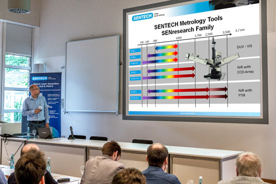
A one day seminar on the topic “Ellipsometry and Reflectometry for the characterization of thin films” was organized by SENTECH in Stuttgart, June 18, 2015. The seminar was focussed on innovations of SENTECH metrology as well as on new developments in science and technology. Invited speakers and SENTECH experts addressed topics from in situ process control, over nanotechnology to photovoltaics.
The talks included guest speakers from different universities and institutions. One of the numerous highlights was the presentation on the topic “In situ measurements in gas environment with ellipsometry” by Brecht Vallaey, University Leuven. He showed how to apply in situ characterizations for different kinds of gases with spectroscopic ellipsometry.
Particularly interesting were the presentations on optical characterization of nanostructured surfaces by Bernd Bodermann from PTB and Ingo Dirnstorfer from Namlab. They showed how to determinate structure parameters from gratings using ellipsometry and special software extensions.
Sessions given by SENTECH experts focussed, for example, on the new SENTECH ALD Real Time Monitor. Dr Kärkkänen, ALD specialist at SENTECH, presented on the effective optimization of ALD processes parameters using the ALD Real Time Monitor.
After the seminar speakers and audience got together for networking and discussion about practical applications and techniques. The SE 800 PV, the SENTECH spectroscopic ellipsometer for photovoltaic research and engineering applications, was demonstrated in a hands-on-ellipsometry. The event created an excellent opportunity for all attendants to share their practical experiences and to network.
Wolfgang Wagenseil, Sales Manager at SENTECH organized this event. He was delighted by the excellent feedback of the participants: “The participants got to know more about the recent advances of charactering materials with SENTECH ellipsometry and reflectometry. They especially enjoyed an intensive discussion about the given presentations afterwards. This will eventually help them to improve their work and researches in the future.” If you want to learn more about upcoming SENTECH seminars contact us here!
Chinese ambassador visits SENTECH
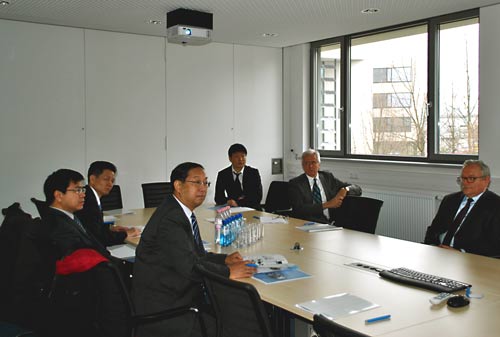
The Chinese ambassador to Germany, His Excellency Shi Mingde visited SENTECH Instruments GmbH on Friday, 10th of March 2015. He was welcomed by Dr Albrecht Krüger, CEO of SENTECH, who introduced the company and its business fields thin film metrology and plasma process technology. Both had a lively conversation about industrial engineering, the innovation strategy of SENTECH products, and their importance for the Chinese market.
His Excellency Shi Mingde was accompanied by his secretary and his counsellor. Dr Krüger welcomed the Chinese delegation at the SENTECH headquarter in Berlin. He gave a presentation on innovations at SENTECH and pointed out the importance of successful cooperation between China and Germany.
His Excellency Mr Shi Mingde highly appreciated the innovative work of SENTECH and underlined the importance of high quality German imports for the Chinese economy. The Chinese delegation enjoyed a walk through SENTECH laboratories and production facilities afterwards. Together with our Chinese distributors SENTECH developed China to one of the key markets for our innovative products. SENTECH would like to thank His Excellency Mr Shi Mingde for the kind visit.If you want to learn more about SENTECH activities in China, contact us here!
ALD Real Time Monitor presented at SEMICON Japan 2014
The annual SEMICON Japan, which brings together experts from economy and science from the semiconductor society, took place from December 3-5 in Tokyo. It was a perfect event to present SENTECHs new ALD Real Time Monitor to the Japanese audience.
SENTECH presented the ALD Real Time Monitor for the first time in Japan. The fast and efficient optimization of atomic layer deposition processes made this new technology especially interesting for visitors at SEMICON Japan.
The SEMICON Japan will be an important event for presenting SENTECHs latest developments also in the upcoming year 2015. We are looking forward to it.
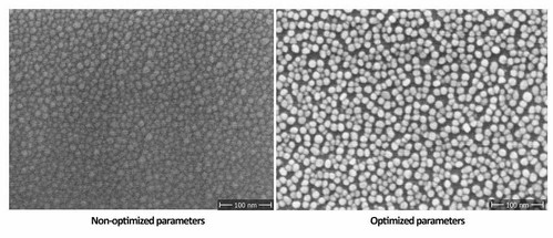
Silver Nanoislands grown by Atomic Layer Deposition, 2014
The new ALD Real Time Monitor was presented at the NRW Nano-Conference (1st-2nd of December 2014). This important conference welcomed its guests to participate the dialogue about opportunities and challenges of nanotechnology.
Optimizing atomic layer deposition processes with SENTECHs newly launched ALD Real Time Monitor was introduced to the German nanotechnology society. This innovative tool features in situ measurement with 40 ms time resolution and an user-friendly software integration into the SENTECH atomic layer deposition system.
SENTECHs presentation focussed on monitoring silver nanoislands growth by plasma enhanced atomic layer deposition using SENTECH ALD. The growth of the silver islands was in situ monitored by the ALD Real Time Monitor, which allows thickness measurements with a sampling time of 40 ms. Dr Irina Kärkkänen, ALD specialist of SENTECH presented the results of the investigations by SENTECH ALD team. “High precision of the measurements and ultra-fast response of the ALD Real Time Monitor allow monitoring of single atomic layer deposition steps. Hence, the process is efficiently optimized in respect to precursor pulse, precursor purge, plasma pulse, and plasma purge. The optimized process parameters lead to silver nanoislands as confirmed by the SEM image.” She concludes: “The ALD Real Time Monitor is a powerful system for in situ process monitoring.”
The ALD Real Time Monitor is perfectly suited for optimized process development, e.g. silver nanoislands growth by plasma enhanced atomic layer deposition. Contact us for more information!
SENTECH at the China ALD Conference 2014
SENTECH new ALD Real Time Monitor was presented in Asia at the 3rd China ALD Conference. For the first time the patented monitor allows the direct monitoring of absorption and desorption processes on the substrate surface during ALD processes within ALD half cycles. Dr. Gargouri, SENTECH specialist for ALD processes, gave a speech during the conference. “Using the ALD Real Time Monitor enables efficient and fast process optimization” Dr Gargouri points out. “With this new tool SENTECH has shown that we have an outstanding Know How in fields of metrology equipment & ALD “.
The 3rd China ALD Conference hold from 16-17 of October 2014 in Shanghai was the ideal event to interchange with the Asian ALD society. It was especially attended by experts from the Asian region. Numerous talks between SENTECH representatives and participants of the conference showed the broad interest in SENTECH ALD equipment and especially in the new Real Time Monitor. For information on SENTECH ALD applications contact us here!
New ALD Real Time Monitor presented at SEMICON Europa 2014
SENTECH offers leading edge plasma process technology equipment for etching and deposition, as well as thin film measurement instrumentation.
With more than 6000 visitors the SEMICON Europa 2014 was the ideal place to introduce SENTECH’s latest development on the field of atomic layer deposition (ALD) – the new ALD Real Time Monitor.
The ALD Real Time Monitor is an insitu measurement tool for adsorption and desorption processes during ALD cycles with millisecond time resolution. The innovative ALD Real Time Monitor is especially designed for fast and efficient process optimization. Additionally, monitoring the film thickness growth the tool is used for end point detection.
The presentation of SENTECH ALD Real Time Monitor drew attention to the newly launched insitu measurement tool and contributed to a successful SEMICON Europa 2014. We are looking forward to the upcoming SEMICON Europa 2015 taking place in Dresden, Germany.
SENTECH is honoured at the „Award for small and medium sized enterprises 2014”
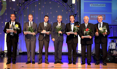
(The 6 finalists, 2nd from right Dr Albrecht Krüger, photo: Boris Löffert)
Because of SENTECH`s constant economic success, and the innovative operating principles we have been honoured at the “Award for small and medium sized enterprises” ("Großer Preis des Mittelstands")in 2014. This famous German award by the Oskar Patzelt foundation dignifies enterprises for their performance in German economy, society, and as well the efforts for their employees.
At the 6th of September, 2014 SENTECH was honoured by the Oskar Patzelt foundation in the district Berlin/Brandenburg. More than 500 guests attended this glamourous event which took place in the Maritim Hotel in Dresden. In total there have been more than 4500 nominees for this highly coveted award.
Dr Albrecht Krüger, CEO of SENTECH Instruments is delighted being rewarded as one of 6 “Finalists 2014”: “I am really glad to receive this honourably award. The appreciation for our constant success and our efforts for the region of Berlin makes me and my team very proud. Especially I want to thank all my employees for their daily enthusiastic work. They make all this possible.”
Following our motto “Erfolg durch Leistung”, we will continue to strengthen the German economy with our entrepreneurial success. If you want to learn more about SENTECH corporate philosophy contact us!
New system for PEALD & ICPECVD in one reactor presented at ThGOT 2014
We proudly presented our new combinatorial system “SIPAR” for PEALD & IC PECVD at the ThGOT conference (Thuringian surface days).
At the ThGOT SENTECH presented the innovative system “SIPAR”, which combines PECVD and PEALD technique in one reactor for depositing moisture barriers. SIPAR complements the wide ranging SENTECH product portfolio with an innovative alternative to cluster systems. In contrast to conventional cluster systems this smart IC PECVD and PEALD combination offers a cost effective solution for the needs of industry and R&D. Combining advantages of SENTECH PEALD, which features excellent conformity and homogeneity, and IC PECVD for high deposition rates at lowest temperatures, the deposition of hybrid multilayer moisture barriers in one reactor is facilitated. Due to the fact that no handling is necessary, processing time will be saved and contamination will be prevented.
The ThGOT has been taking place from 2. untill 4. of September in Leipzig, Germany. It was the 10th anniversary of this popular conference and many visitors from industry and science attended the various presentations and poster sessions. SENTECH participated on the event with a booth as well as with introducing the newly developed combinatorial system for PEALD and IC PECVD “SIPAR” for depositing moisture barriers.
“The interest in ALD has grown enormously in the last years, this can be seen from the increasing number of presentations on the topic at ThGOT” Dr Gargouri, one of SENTECH`s plasma specialists resumes. If you are interested in more details of our new IC PECVD & PEALD system SIPAR, please contact us here!
Application-oriented thin film measurement seminar by SENTECH 2015
SENTECH as a worldwide leader in thin film measurement and plasma process technology organizes application oriented seminars on a regular basis. The most recent seminar “Ellipsometry and Reflectometry for characterizing thin films” was on thin film measurement. More than 20 participants mainly from industry as well as SENTECH users were part of the audience. The seminar took place on 24th of June, 2014 in Munich.
Recent topics of thin film measurement like organic layers and organic solar cells were discussed within the numerous presentations. SENTECH`s latest developments – the measurement of 16 Mueller-Matrix-Elements and scatterometry – were especially focused on. One of the outstanding highlights of the seminar was the presentation on “Measuring optical properties of organic layers for characterizing OLEDs” by Christian Mayr from the University of Augsburg. In this application, spectroscopic ellipsometry is applied to estimate the later efficiency of an organic LED. A presentation by M. Baklanov from IMEC addressed the “characterization of coatings with huge internal surfaces by using ellipsometry”.
In addition to the talks, the audience highly appreciated the demonstration of SENTECH`s ellipsometers and reflectometers for thin film measurement. SENTECH demonstrated how the step scan analysator in combination with high sensitive detector-arrays allows the measurement of rough and textured surfaces.
The active exchange with users and experts in thin film measurement is an important aspect for SENTECH. Customer oriented research and development in thin film measurement as well as in plasma process technology is our dedication. Hence, we are organizing innovative seminars several times a year. If you want to learn more about upcoming SENTECH Seminars and workshops, contact us!
“Plasma Etching & Deposition” Seminar in China enjoyed great popularity, 2014
A one day technical plasma seminar was given by SENTECH in cooperation with Beijing Oriental Jicheng Co. Ltd in Shanghai on June 20th, 2014. The Chinese institute SIMIT (Shanghai Institute of Microsystem and Information Technology) hosted this annual event, which gained the attention of many students, scientists and experts from industry, like it had the previous years. More than 60 participants have joined this informative one day event, which contained advanced information about plasma etching & deposition with a focus on new trends in plasma etching, PECVD and ALD.
Expert speakers from SENTECH and from scientific organizations in China focussed on recent plasma process topics like deep silicon plasma etching processes and applications. Furthermore, ICP plasma etching of III-V compounds and in situ ellipsometry for ALD systems were covered. The technical program of this free of charge seminar was set up to stimulate customers´ interests in SENTECH´s recent technical advances and to support plasma users in their practical work. Between the presentations lively discussions about specific technical details as well as the suitability of ICP processes for creating solutions to future application challenges came up. Special interest was on ICP plasma deposition at low temperatures for temperature sensitive substrates. SENTECH was glad to underline that high quality ICPECVD film deposition temperatures lower than 130° C are feasible with our ICP plasma deposition tools.
Evaluating the participants’ feedback confirmed the positive impressions that the SENTECH presenters had experienced during the event. There was a very positive feedback to context and standard of all presentations. This stimulates SENTECH to continue organizing workshops and events around plasma etching and deposition topics. “Hence SENTECH is planning to institutionalize more of those workshops on plasma topics on a regular basis” Mr Gruska, CMO of SENTECH Instruments reveals. If you want to learn more about SENTECH plasma etching and PECVD Seminars contact us!
Efficient spectroscopic ellipsometers for PV presented by SENTECH at SNEC 2014
The SNEC PV Power Expo 2014 is one of the world leading photovoltaic exhibitions and took place on May 20-22 in Shanghai, China. At 2150,000 sqm more than 1500 exhibitors presented innovative solutions and new products for the production of clean and sustainable energy. This PV trade show is one of the best opportunities to meet experts and suppliers from the PV industry and to see PV manufacturing facilies, PV materials and cells as well as every other section of the PV market.
The focus of SENTECH was on our attractive and innovative spectroscopic ellipsometers for PV, SE 800 PV and SE 850 PV. Their high measurement sensitivity, depolarization correction, and special light collecting optics make our SE 800 PV/SE 850 PV ideal tools for photovoltaic applications.
On the SNEC 2014 SENTECH gained very good response for those efficient spectroscopic ellipsometers. In general the photovoltaic market demands for more modern applications to increase the efficiency of next generation solar cells. Those SENTECH PV ellipsometers are perfectly able to satisfy those prospects.
SENTECH wants to thank all customers and the numerous interested parties for visiting us at the SNEC Show 2014. We are looking forward to great cooperations and to a successful year 2014 in Photovoltaics.
Invitation to the SENTECH Seminar: “Ellipsometry and Reflectometry for characterizing thin films 2014”
SENTECH as a worldwide leader in thin film measurement and plasma process technology is glad to announce a one day seminar “Ellipsometry and Reflectometry for characterizing thin films”. The Seminar will take place on June 24th, 2014, at the NOVOTEL Hotel “München Messe” in Munich-Riem.
This innovative application oriented seminar focuses on ellipsometry and reflectometry for thin film analysis. Contributions from experts of different research areas will cover the characterization of organic layers like OLED´s or organic solar cells. Furthermore the characterization of large surface materials and photovoltaics will be emphasized.
SENTECH experts will give presentations on our newly developed spectroscopic ellipsometers and SpectraRay software for thin film measurement. We will be glad to demonstrate our ellipsometers and reflectometers during the Seminar.
All presentations of the seminar "Ellipsometry and Reflectometry" are available to the participants after the seminar.
The seminar program can be downloaded here: Program SENTECH Thin Film Seminar 2014 . To register for this event please use our Registration Form.
Please use the registration form to register as soon as possible, as the number of participants is limited to 30. Attendance fee: 180,00 € incl. VAT.
Please send your registration to sales@sentech.de or via fax to +49 89 897 9607-22. For further questions please contact SENTECH via telephone: +49 89 897 9607-0.
SENTECH at the 8th Workshop Ellipsometry in Dresden 2014
SENTECH Instruments is a leading supplier of plasma process technology equipment for etching and deposition and thin film metrology instruments based on ellipsometry.
The communication with our customers and users is a very important aspect of the service activities of SENTECH Instruments. As we are supplying and developing high quality metrology equipment like our SENresearch we are always aimed to reach highest satisfaction of our customers. Therefore we keep in touch with our users by attending events like the Ellipsometer Workshop 2014 in Dresden.
This Workshop took place in March at the Leibniz Institute of Polymer Research. Scientists and engineers from the metrology society discussed recent developments in science, technology and application for Ellipsometry. The main focus of this workshop was on experiments using Müller Matrix analysis. For this field of study SENTECH provides a smart option for the SENresearch tools for detecting all 16 different Müller-Matrix-Elements.
SENTECH not only took part in these discussions but also contributed two posters which were specified on recent developments of ellipsometric applications at SENTECH. On the first poster the application of in situ monitoring for plasma processing, especially atomic layer deposition ALD, was presented. With SENTECH inline metrology tools layer by layer growth can be resolved with single cycle resolution. Hence ALD deposition can be analysed and optimized on a cycle basis with SENTECH spectroscopic and laser ellipsometers. In the second poster the analysis of graphene flakes was shown. Counting and mapping graphene monolayers is enabled by SENTECH thin film measurement tools.
We are proud of receiving very positive feedback concerning the performance of our metrology devices. The enthusiasm of our customers empowers us to maintain our broad customer service as well as to enlarge those activities to always meet the requirements and needs of all users of SENTECH metrology equipment. If you need further service support on our spectroscopic ellipsometers contact us here!
SENTECH at SEMICON China 2014
Also in year 2014 SENTECH was part of the SEMICON China to present all recent developments in ICP plasma etching and deposition, real time monitoring of ALD processes and thin film metrology to the members of the semiconductor society. Organized by SEMI and CECC the SEMICON China is one of the leading exhibitions for microelectronic technology. The exhibition took place from March 18-20.
SENTECH is glad to announce that our products attracted widest interest. Especially our solutions for the deposition and measurement of very thin films were discussed intensively. SENTECH`s booth in hall N2 was well frequented and we thank all our guests for visiting us and for all promising conversations. The good connections we build up in Shanghai will be continued after the exhibition.
The next SEMICON 2015 will take place in Shanghai as well and SENTECH is looking forward to be part of it again. For any further sales or service support contact us here!
SENTECH Seminar: “Plasma Process Technology” 2014
SENTECH offers leading edge plasma process technology equipment for etching and deposition and thin film measurement instrumentation based on ellipsometry. The advanced SENTECH plasma equipment is based on the inductively coupled plasma source PTSA (planar triple spiral antenna) which was developed by SENTECH for low damage and high rate etching and deposition. The latest product development at SENTECH expands the ICPECVD product line by ALD and plasma enhanced ALD systems.
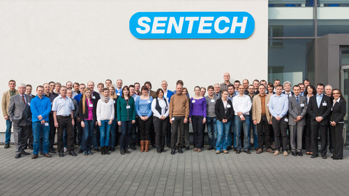
SENTECH has organized a seminar on Plasma Process Technology on February 27, 2014 held at SENTECH Instruments in Berlin Adlershof. The seminar offers great networking opportunities for specialists of the thin film plasma community. The Seminar was already the 8th plasma seminar and attracted more than 50 specialists from industry, research institutions and universities.
The group picture above was taken during lunch break in front of the SENTECH building in Berlin Adlershof:
At the seminar recent developments in plasma etching, in plasma enhanced deposition and in atomic layer deposition were presented by invited speakers and by specialists from SENTECH Instruments. One of the outstanding highlights of this event was the presentation on ALD combined with PECVD of Mr Bülow from TU Brunswick. The combination of ALD and PECVD in one SENTECH tool enables remarkable OLED encapsulation.
A presentation on Si etching application held by Mr Voigt from Leibnitz Institute for Photonic Technologies, Jena underlined the high efficiency of Si etching with SENTECH ICP plasma systems. Another highlight on graphene entitled “Challenges in graphene synthesis and semiconductor/graphene structures” was presented by Mr Lukosius from IHP Frankfurt/Oder. Other presentations reported on product technologies and application highlights.
Finally the participants of the seminar were invited to visit SENTECH’s application laboratories and manufacturing facility. Quoting some of the visitors, the seminar was described as very innovative and inspiring, the excellent networking opportunities were specially complimented.
Motivated by the success of the seminar on plasma process technology in 2014, SENTECH considers to continue to offer seminars dedicated to SENTECH Plasma Process Technology. The presentations and information are available by SENTECH upon request.
SENTECH Plasma Process Technology Seminar 2014
In good tradition SENTECH is glad to announce its annual Plasma Seminar which takes place on Thursday, February 27th, 2014 at SENTECH Instruments GmbH, Schwarzschildstraße 2, Berlin Adlershof.
As the global interest in Nanotechnology is growing, we want to get our participants introduced to new topics in fields of deposition and etching combined with recent examples. Invited speakers will focus on topics such as the deposition through ALD and PE-ALD, the etching of micro- and nanostructures in Si, the manufacturing of graphene films and the deposition of passivation and encapsulation films through IC PECVD and ALD. The whole Seminar Program can be downloaded here: Programme_SENTECH Plasma Seminar . If you want to participate please send this Registration for SENTECH`s Plasma Process Technology Seminar to: sales@sentech.de
After the seminar there will be a presentation of the SENTECH application laboratories and its production facilities. The whole material of this seminar will be provided for all participants.
For further information don`t hesitate to contact us or call: +49 89 8979607-0
(SENTECH`s Plasma Processtechnology Seminar 2013)
SENTECH seminar in Beijing, China 2013
On 20th November 2013 SENTECH presented the first seminar for Plasma Process Technology and Analysis of Thin Films in Beijing, China. Over 150 participants including customers and potential buyers took part at the seminar which was held at the National Center of Nanoscience and Technology China (NCNST). Speakers from NCNST, Zhejiang University China and SENTECH discussed about the latest results in ICP-RIE, ICPECVD, ALD and Ellipsometry. We want to thank all participants for their active attendance and many fruitful discussions. Especially we want to thank all people of the NCNST and the SENTECH China Sales Office for their great support.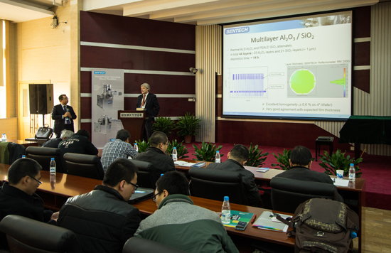


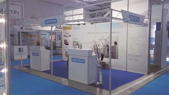
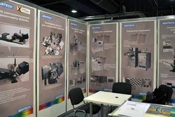
SENTECH at SEMICON Europa 2013
SENTECH presented its latest products for Thin Film Metrology and Plasma Enhanced Atomic Layer Deposition at the 37th SEMICON Europa 2013. The exhibition took place from October 8th to 10th 2013 in Dresden, Germany. With over 350 exhibitors the SEMICON Europa is the leading forum for semiconductors and microelectronics manufacturing in Europa. In 2014 the SEMICON Europa will take place in Grenoble, France and SENTECH will be part of it once again. We want to thank our customers and numerous interested persons for their visits and promising conversations. For sales and service support please don’t hesitate to contact us.
Spectroscopic Ellipsometer for Singapurian training facility 2013
 SENTECH Instruments delivered the next spectroscopic ellipsometer SENresearch to Singapore.
It is the first spectroscopic ellipsometer for some time that has gone to a Singaporean training facility. The thin film measurement device is now installed at Ngee Ann Polytechnic (NP), one of Singapore’s leading institutions of higher learning located in Clementi.
The customer selected an instrument with the latest software version of SpectraRay/3— SENTECH’s advanced spectroscopic ellipsometry software.
Additionally, the customer benefits from one notable advantage: SENTECH’s service office Asia is located in Singapore and will serve directly on site.
July 2013
SENTECH sponsored E-MRS 2013 Spring Meeting

In May 2013, the E-MRS Spring Meeting took place in Strasbourg, France. It included 24 parallel symposia, one plenary session, and one exhibition.
SENTECH participated as gold sponsor of the symposium A called “Energy conversion applications of atomic layer deposition”. This symposium was organized by the Inorganic Chemistry Chair of the University of Erlangen-Nürnberg (Germany), by the EMPA Swiss Federal Laboratories for Materials Science and Technology (Switzerland), the Energy and Environment Department of IMRA Europe SAS (France), and the MPI for the Science of Light (Germany).
The symposium focused on the development and exploitation of atomic layer deposition (ALD) methods enabling the inter-conversion of solar, electric, and chemical forms of energy. The possibility offered by ALD to coat complex structured substrate architectures with functional layers was the underlying theme.
Thereby, hot topics were covered such as: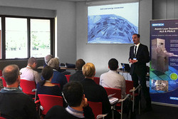
- ALD passivation/protection layers, ultrathin inert layers —
for improved ageing or less recombination - Ion-conducting ceramics by ALD,
electronic insulators conducting protons or lithium ions - Thin solid dye layers by ALD,
“extremely thin absorber” concept in photovoltaics - Transparent conducting oxides by ALD, optimization of electrical and optical properties of novel TCOs at low thermal budgets
The proceedings of the symposium will be published in the Beilstein Journal of Nanotechnology, a publication of the Beilstein Institute.
June 2013
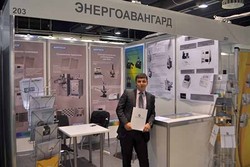
SENTECH at SEMICON Russia 2013
From June 4 to 6, SENTECH Instruments participated in SEMICON Russia 2013. This trade fair in Moscow is the key event for semiconductor production, equipment, materials and service in Russia, and attracted more than 2,500 visitors.
SENTECH participated in the exhibition together with its long-standing Russian distributor EnergoAvangard. Latest applications and developments were presented in the fields of RIE etching, PECVD deposition, ALD atomic layer deposition, and thin film measurement.
We want to thank our customers and numerous interested persons for their visits and promising conversations. We hope to continue these good co-operations and, furthermore, increase our success in the strongly growing market of Russia.


June 2013
SENTECH’s Plasma Process Solution at SEMICON China 2013
From March 19 to 21, SENTECH Instruments participated in SEMICON China 2013. It is the key trade show for semiconductor production, equipment, materials and service in Shanghai, China, and attracted more than 40,000 visitors.
This Year, SENTECH put special emphasis on the presentation the fields of ICP/RIE plasma etching, IC/PECVD plasma deposition, and atomic layer deposition (ALD). Latest applications, process developments, and special system configurations were presented.
Together with its Chinese Sales Office SENTECH participated in the official German Pavilion. Additionally, our distributor Beijing Oriental Jicheng was present with an own booth. SENTECH wants to thank our numerous visitors for the promising conversations especially about up-to-date plasma process applications. Subsequent to this event, we expect further increase of our business in China for the next 12 months.

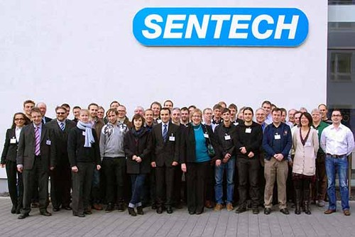
Seminar "Plasma Process Technology" at SENTECH 2013

More than 50 participants from industry, universities, and scientific institutions participated in SENTECH’s seminar “Plasma Process Technology” on February 28, 2013, in Berlin, Germany. The Seminar focused on issues of topical interest, including GaN processing, silicon nanostructuring, low temperature deposition of SiN, graphene components, and ALD barrier layers. One special highlight was a report on the deposition of low hydrogen concentration SiN films at
Another highlight of the seminar was the visit to SENTECH’s manufacturing facilities and well-equipped application laboratories for plasma process technology and thin film measurement. The seminar received very positive ratings and will be continued with up-to-date topics in 2014. The picture shows the participants of the seminar in front of the SENTECH Instruments company building in Berlin.
SENTECH Instruments is a worldwide leader in plasma process technology equipment. SENTECH develops, manufactures, and sells advanced plasma etch- and deposition systems based on its proprietary PTSA-ICP plasma source. The systems offer low damage, high rate, and low temperature processing for device manufacturing and
February 2013
Invitation: Seminar "Plasma Process Technology" at SENTECH 2013

Nanotechnology is a key application area of state of the art etch and deposition processes. Experts and users interested in up-to-date and practice-related developments in the field of plasma process technology are cordially invited to visit SENTECH’s coming Seminar Plasma Prozesstechnologie.
The application-oriented seminar takes place on Thursday, February 28, 2013, at SENTECH Instruments GmbH in Berlin-Adlershof, Schwarzschildstraße 2. Competent referents will illustrate various application fields of modern etch and deposition technologies using specific examples. Additionally, experts from SENTECH are going to present latest developments and point out according applications.
Nano structuring of silicon for photovoltaics and sensors is one of the main topic during the seminar. Further, nano-scaled deposition of very thin films by thermal and plasma enhanced atomic layer deposition (ALD) for e.g. OLED technology is focused. Another highlight is a presentation about modern electronic devices based on graphene. Following the presentations, the plasma application laboratory of SENTECH might be visited.
The Seminar Program can be downloaded here.
For additional questions, please contact us via telephone: +49 89 8979607-0
or e-mail: sales@sentech.de.
January 2013
Customer-oriented application support: SENTECH’s Metrology Application Laboratory 2013
A deep insight into the functionality of SENTECH equipment is given by a visit to our application laboratories for thin film measurement and plasma process technology. These well-equipped application areas are designed for the processing of customer samples to develop solutions according to the customers’ requirements. Our ambitious application team consists of eight highly qualified experts. They provide device demonstrations and customized user training with the equipment in operation. Services like contract measurements are carried out as well. Furthermore, our experts generalize interesting tasks to open up new fields of application for our products.
 Metrology Application Laboratory

The Metrology Application Laboratory is equipped with measuring instrumentation covering a wide range of applications. Spectroscopic ellipsometers with different configurations are provided for the spectral range from
Please contact us for more information.
November 2012
First Plasma Deposition System installed in Australia 2012

SENTECH Instruments sells its products worldwide. Now, the first plasma deposition system has been installed at the University of Western Australia in Perth by SENTECH Service Asia. Support was provided by our Australian distributor KKI International.
In Perth, the School of Electrical, Electronic & Computer Engineering develops components that are mainly used for optical data transmission and telecommunications in the infrared. SENTECH ICPECVD system SI 500 D is used for the deposition of low stress silicon nitride and silicon oxide films.
The SI 500 D represents the leading edge for plasma enhanced chemical vapor deposition of dielectric films. The system is based on SENTECH proprietary Planar Triple Spiral Antenna (PTSA) ICP plasma source for exceptional plasma properties like high density, low ion energy, and low pressure. Low etch rate, high breakdown voltage, low stress, no damage of substrate, very low interface state density, and depositions down to temperatures of less than
Please contact us for more information.
September 2012
Training for Russian service manager 2012

To ensure constant highly qualified service for our customers, SENTECH worldwide distributors and service technicians are trained on-device within our manufacturing and application environment in Berlin, Germany. Recently, a service engineer from EnergoAvangard – our distribution and service partner in Russia – visited SENTECH for a two-weeks training session.
The focus of the training was placed on installation, service, and application support especially for SENTECH spectroscopic ellipsometers. It is the goal to qualify the service engineers of EnergoAvangard for installation on the customers’ site without time delays. Additionally, EnergoAvangard is always the first point of contact for any questions from customers in Russia, providing best application support and technical service without language barriers.
Generally, SENTECH places great importance on the worldwide presence of well-trained distributors and service technicians. By now, we have been cooperating with EnergoAvangard for more than 10 years in mutual confidence and success. Especially during the last years, cooperation has intensified due to the strongly growing market and the success in selling our products in Russia.
August 2012
Customer-oriented application support: SENTECH’s Plasma Application Laboratory 2012
A deep insight into the functionality of SENTECH equipment is given by a visit to our application laboratories for thin film measurement and plasma process technology. These well-equipped application areas are designed for the processing of customer samples to develop solutions according to the customers’ requirements. Our ambitious application team consists of eight highly qualified experts. They provide device demonstrations and customized user training with the equipment in operation. Services like contract measurements are carried out as well. Furthermore, our experts generalize interesting tasks to open up new fields of application for our products.
 Plasma Application Laboratory
The Plasma Application Laboratory provides equipment for a wide range of plasma etching and deposition processes. ICP-RIE plasma etchers allow for fluorine etch processes, methane hydrogen processes, and chlorine chemistry. Deposition of dielectric layers can be done by a PECVD system or at much lower temperatures by an ICPECVD system. The ALD system is designed for thermal and plasma enhanced atomic layer deposition processes. Additionally, a spectroscopic ellipsometer, a scanning electron microscope, and a profilometer are provided for sample characterization. In this application area, our plasma application experts develop new processes for
Please contact us for more information.
July 2012
SenSol Haze ordered by Samsung SDI and Oerlikon/TEL 2012
The automated mapping system SenSol Haze is still in high demand. Within one month, SENTECH Instruments has won two contracts: Samsung SDI from South Korea as well as Oerlikon Solar / Tokyo Electron Limited from Japan have ordered the large area inspection tool.
These new big orders represent a further step forward into the Asian market. As one of the leading suppliers of thin film metrology tools in the field of photovoltaics, SENTECH is seeing an outstanding potential in this growing market.
Samsung SDI is a world’s leader in the display and energy businesses, mainly based on lithium-ion systems. To increase their efforts in the eco-friendly and clean energy area, the company has taken over the promising photovoltaic business from Samsung Electronics in 2011. Similarly, Tokyo Electron Limited (TEL) — a leading global supplier of semiconductor production equipment — has focused its activities even more on the photovoltaic cell industry by the recent takeover of Oerlikon Solar.
Both companies will deploy the SenSol Haze for quality control in the manufacturing of thin film solar cells. The system offers automated uniformity mapping of film thickness and spectrally resolved Haze H(λ) on glass sheets of all standard glass sizes.
June 2012
SENTECH at SEMICON Russia 2012
SENTECH successfully participated in SEMICON Russia 2012, prime exhibition of microelectronics, semiconductor manufacturing equipment, optics, and nanotechnology in Moscow from May 15–16, together with its local distributor partner EnergoAvangard.
Dr. Michael Arens, head of plasma process technology department at SENTECH Instruments, presented latest developments like the SENTECH Atomic Layer Deposition system. Due to the pleasingly high level of demand at this exhibition, SENTECH is expecting growing sales of plasma equipment in Russia in the months ahead.
Mr. Sergey Verzhbitskiy from EnergoAvangard invests much energy in supporting our customers on site. For local sales and service support in Russia please contact him directly.
May 2012
On-site Distributor Meeting and Training 2012

Worldwide distributors of SENTECH products have visited Berlin from April 23th to 27th, 2012, for sales meeting, product education, and on-site training.
New developments like the Atomic Layer Deposition (ALD) system were presented by SENTECH experts. Additionally, the local SENTECH representatives got the opportunity for practical training with SENTECH equipment to improve their sales and service activities.
During the conference, latest developments in the local markets have been discussed. 2011 was a successful year for SENTECH distributors all over the world. However, growing tensions especially on the global PV market require realignments. So, the cooperation partners have made important decisions to put a greater emphasis on SENTECH strengths and unique selling propositions. For future, the salesmen expect significant progress from efforts to open up new market niches.
April 2012
A robot on the way to World Championship 2012
 The little robot is speeding through the glass labyrinth. Light sensors are following the black line painted on the ground. Obstacles in its path are detected by touch sensors from a computer mouse. The inclination sensor signalizes a steep ramp, but the crawler manages the slope. Having reached the summit, the biggest task is waiting for the small vehicle: to detect and rescue the victim – represented by a box.
All these challenges, the ArcheRobots have mastered successfully during the RoboCup GermanOpen 2012 in Magdeburg and, therefore, made it into the top five teams that are qualified for the RoboCup World Championship taking place in Mexico-City in June 2012.
For many years, SENTECH Instruments is cooperating with schools and training institutions to support young people in putting their research ideas into practice. Now, the company is sponsoring four boys from the Archenhold-Oberschule Berlin who participate in the international RoboCup competition.
The ArcheRobot team has started in the category Rescue Primary A. Its self-constructed robot had to solve problems that are faced by usual rescue robots – to search for victims independently on rough terrains. More than a half year of developing, experimenting, and programming is concealed behind the masterly performance of the four students from Berlin. Nevertheless, the great success was worth the effort.
Postscript:
They have made it to world championship – Within the individual competition, the ArcheRobots have reached the 7th place what qualified them for the Super Team Challenge. Here, together with a Japanese team, the four boys from Berlin conquered the World Champion's title.
April 2012
International Recognition for SENTECH 2012

With the Adlershof Science and Technology Park, the BiotechPark Berlin-Buch, and the Charlottenburg Business Incubator and Innovation Centre, Berlin has a very good reputation throughout the world. This reputation is due to medium-sized companies like SENTECH Instruments that use local resources and cooperation to build international success upon it. Now, the Berlin technology park model has attracted some extremely high level representatives from SKOLKOVO, one of the leading development projects in Russia.
The village Skolkovo with a population of just a few hundred is located some kilometers southwest of Moscow. Since 2011, an extensive science and technology city is coming into being here — initiated under the personal authority of Dmitry Medvedev, president of the Russian Federation at that time. The whole development project is supported by an international science consortium called SKOLKOVO Advisory Board. Its importance is shown by the staffing of this commission with the Nobel Laureates Roger Kornberg and Zhores I. Alferov.

Invited by two of its German members, Prof. Ganten (Charité) and Prof. Bimberg (TU Berlin), the committee has visited the great technology parks of Berlin at the beginning of March 2012, looking for inspiring role models for SKOLKOVO. SENTECH Instruments was one of the few selected institutions for company visits in Adlershof. According to its long-standing and successful research and development, especially in the field of plasma process technology, SENTECH is proud to serve as a best practice example for companies in Skolkovo. On the basis of this meeting, SENTECH intends to pursue future cooperation with the growing Russian technology location.
March 2012
New Service Support in Asia, 2012

In order to expand our service in Asia, we are pleased to announce the establishment of a new service support located in Singapore.
Mr. Roland Kögel, a long-standing employee of SENTECH Instruments in Berlin, Germany, is providing fast and easy technical service by reducing former constrains due to distances and time differences. Based on his experience with the whole range of SENTECH metrology and plasma process products, we will now provide an enhanced customer and distributor support with this new branch. Mr. Kögel has already begun his work in Asia.
Contact:
SENTECH Service Support Asia
Mr. Roland Kögel
Singapore
Mobil: +65 8181 7540
E-Mail: service@sentech.de
For our worldwide service support please see here.
March 2012
Successful research in the field of Plasma Process Technology, 2012
 EPILOGOS — behind this name lies a highly efficient microwave plasma source that enables the deposition of perfectly thin layers. It is especially designed for plasma enhanced deposition. SENTECH has developed this future-oriented plasma source together with its long-standing research partner Ferdinand-Braun-Institut (FBH) within a project funded by the Investitionsbank Berlin (IBB). EPILOGOS serves as groundwork for SENTECH’s current investigations in the field of plasma-enhanced atomic layer deposition (PEALD). It is only one in a whole series of projects in the field of plasma process technology that are currently pursued by SENTECH experts.
The Innovative Regional Growth Core WideBaSe, funded by the BMBF, is dealing with the investigation of wide bandgap semiconductors. The growth core includes several joint projects. SENTECH is involved in three of them together with the FBH, the TU Berlin, and other companies from the German capital. The projects focus on deposition of UV-stable AR coatings by ICPECVD and ALD, on etching of coupling structures for focusable UV-LEDs, and on passivation and utilization of AlGaN transistors for power amplifiers and oscillators.
The European Union is funding an international project investigating the fabrication of Negative Index Materials by Nano Imprint Lithography (NimNil). Here, together with companies from Austria, Serbia, Greece, Italy, and Germany, SENTECH is investigating the manufacturing of negative index materials (NIMs) using adapted etching processes. Furthermore, it contributes its many years of experience in metrology to the optical characterization of NIMs by SENTECH ellipsometers.
For more information please see our projects or contact us.
February 2012
“Cool” nano electronics by CoolMaskMetro, 2011
The development of power saving “cool” nano electronics is the basis for a massive increase of energy efficiency in the information and communications technology (ICT) sector.
The project CoolMaskMetro is funded by the Federal Ministry of Education and Research as well as by the European Regional Development Fund (ERDF) until 2014. It is part of the leading-edge cluster Cool Silicon and aims at the development of exact metrology tools for masks in nano chip production. SENTECH brings in its long-term experiences of spectroscopic ellipsometry to develop an economically attractive inspection tool together with an international consortium.
In chip production, structures of chip masks are transferred to silicon wafers within a photolithographic process. To double the energy efficiency of the finished chip, the high-end photo mask manufacturing process has to be improved. Especially quality factors like roughness and regularity of the line structures determine mask quality. Due to the fact that currently available monitoring techniques supply too little resolution of less than 100 μm, CoolMaskMetro is developing a highest-resolution measurement tool based on a spectroscopic ellipsometer for continuous photo mask production monitoring.
For more information about this topic, please contact us.
January 2011
SENDURO® training for Russian customers, 2011

For three days, two guests from JSC “OKB-Planeta”, Velikiy Novgorod, Russia, have been visiting SENTECH Instruments to be trained at their own spectroscopic ellipsometer SENDURO® before delivery. Thereby, the number of SENTECH automated measurement tools installed at Russian companies is continuously growing.
SENTECH fully automated spectroscopic ellipsometer SENDURO® allows for total analyses of samples in only a few seconds. Its compact housing and its high sample throughput rate make the SENDURO® perfectly suitable for production environment.
JSC “OKB-Planeta” develops, designs, and manufactures, inter alia, thin film products (hybrid integrated structures) and electronic devices (semiconductors). The SENDURO® will be primarily used for production monitoring, but also for
Due to minimized installation effort and automated sample alignment, the SENDURO® is very user-friendly and comfortable to handle. So, after a short introduction to hardware and installation, the training has been focused on the included software package comprising SpectraRay/3, SENTECH spectroscopic ellipsometer software with interactive and recipe mode, FTP software, and mapping software. The guests from Russia were introduced not only to operate the SENDURO® and to apply the SpectraRay/3 to sample analysis, but also to carry out technical service issues as well.
December 2011
Plasma Process Technology Seminar 2011

The Plasma Process Technology Seminar 2011 was held on November 22, 2011, at SENTECH Instruments in Berlin-Adlershof. More than 45 guests from well-known companies, universities, and research centers participated in this application oriented seminar.
Competent experienced experts in plasma process technology and SENTECH in-house specialists presented the latest developments and technical solutions in the field of plasma etching and deposition. Current challenges in nano etching for micro optics, laser fabrication, and microelectronics as well as very thin film deposition by ICPECVD and ALD were discussed. Special emphasis was placed on SENTECH’s latest development in PEALD. Subsequent to the presentations, all guests were invited to visit SENTECH’s manufacturing area as well as the application laboratories to get a more practical insight.
Speakers were:
- Nico Ketteniß (Department of GaN Device Technology, RWTH Aachen)
- Ernst-Bernhard Kley (Institute of Applied Physics, Friedrich Schiller University, Jena)
- Lutz Müller (Center for Micro- and Nanotechnologies, Ilmenau University of Technology)
- Thomas Wächtler (Fraunhofer Institute for Electronic Nano Systems, Chemnitz)
- Robert Weih (Chair for Technical Physics, University of Würzburg)
- Michael Arens, Hassan Gargouri, Ralph-Stephan Unger, Prof. Klaus Wandel, Xuemei Wang (SENTECH Instruments, Berlin)
For more information about this exciting seminar and for presentation materials, please contact us.
November 2011
Activation of the new SENTECH website, 2011

SENTECH proudly announces the launch of its completely renewed web presence. After more than a half year of preparation, the new website comprises updated company and product descriptions in a modern, pleasing design.
The reworked structure provides increased usability. SENTECH product areas are divided into three groups — plasma process technology, thin film metrology, and metrology for photovoltaics — to allow interested parties to browse more intuitively. The easiest and quickest way to navigate through our website is by using the drop down menu navigation on the top of every page.
According to nowadays browsing routines, the new web presence bases more on visual than on textual information. Revising the further website, redundant information was eliminated and texts were shortened to get quickly to the point. Many pictures, links, and visual effects relieve the search for details.
Up-to-date announcements like product launches or current vacancies are easily accessible. Our latest news as well as forthcoming and previous events inform about the development of our company. Photo boxes and individualized download areas for special guests and customers offer a deeper insight. Suitable worldwide contact partners are given for every issue relating to our products — additionally, you may use our contact form to contact SENTECH directly.
For any comment or question you may have about the new SENTECH web presence, please do not hesitate to contact marketing.org@sentech.de.
November 2011
SENTECH selected as supplier for Oerlikon Solar, 2011

Oerlikon Solar, Switzerland, is convinced of the SENTECH SenSol Haze for quality control of TCO films in PV manufacturing of thin film solar cells. This inspection tool offers uniformity mapping of film thickness, spectrally resolved Haze H(λ) and sheet resistance on glass sheets of all standard glass sizes.
Oerlikon, a leading provider of thin film PV manufacturing equipment for the mass production of thin film silicon solar modules, is now one of our key reference customers of the SenSol H. They use the SenSol H for mapping the spectrally resolved haze and thickness of TCO layers on glass panels to drastically reduce the system service downtime. The company recommends the SenSol H as quality control tool to its international customers.
September 2011
Entering the Chinese market of thin film metrology, 2011

In April 2011, SENTECH was awarded a new contract of a SenSol H mapping system for the offline analysis of large area thin film solar cells. It is the first system sold into the Chinese market.
The new big order opens up outstanding perspectives on this growing market as SENTECH is one of the leading suppliers of thin film metrology tools in the field of photovoltaics.
Please contact us for more information.
April 2011
SENTECH received Megawatt Honor Award, 2011

We are proud to announce that SENTECH spectroscopic ellipsometer SE 800 PV has been awarded with the Megawatt Honor Award at the SNEC PV Conference and Exhibition 2011 in Shanghai China in the category “Top 10 Highlights”. The award underlines the success of SENTECH Instruments of being a leading provider of spectroscopic ellipsometers for measurements of thickness and refractive index of anti-reflective coatings on silicon solar cells.
Please contact us for more information.
March 2011
2010 was very successful
2010 was a very successful year for SENTECH activities in photovoltaics, especially in China and Taiwan. More than 300 laser ellipsometers are now in the field and help our customers to monitor film thickness and refractive index of AR coatings on textured Si solar cells.
2011 SENTECH further strengthens its activity in Asia, especially in Korea. SENTECH will have its own booth at the Expo Solar 2011, February 16-18, in Korea and invites all visitors interested in thin films metrology for wafer based and thin film solar cells. Together with our new partner ELIM GLOBAL Co., Ltd. we want to increase our market share in Korea and offer an excellent application and service support.
February 2011
Plasma process technology seminar at SENTECH Instruments, 2010
The application-oriented seminar „plasma process technology” was held on November 16, 2010 in the new company building of SENTECH Instruments in Berlin-Adlershof. Competent experts from research and development presented latest etching and deposition technologies and explained their use in various examples. Furthermore employees of SENTECH Instruments focused on technical solutions, reported on new developments for ICP-RIE, RIE and PECVD technologies and presented applications to the 30 participants of the seminar.
Speakers were: Philip Moser from TU Berlin, Mohammed Aid Mansur Al-Suleimann from TU Braunschweig, Dr. Franz Müller from PTB Braunschweig and Robert Zierold from University Hamburg.
December 2010
SENTECH celebrated 20th anniversary and completion of the new company building, 2010

On September 30, 2010 SENTECH Instruments celebrated its 20th anniversary as well as the completion of the new company building in Schwarzschildstraße 2.
About 100 guests from Germany and from abroad attended to the celebration and got to know the new house but also the company.
Speeches were held by Dr. Jens-Peter Heuer (Secretary of State of economy, technology and women), the general contractor of the house Joachim Gericke (Gericke-Bau GmbH) and Dr. Peer Ambrée (WISTA-MANAGEMENT GmbH).
Afterwards the guests were shown around the new company building. The celebration was musically entertained by the band "The Neighbors".
SENTECH would like to thank all business partners, suppliers, distributors and friends for successful teamwork. We’re looking forward to continuing our promising cooperation.
October 2010
Harald Wolf visits SENTECH at the 25th EU PVSEC, 2010

The world’s biggest photovoltaic conference and exhibition, the EU PVSEC, took place from September 6-9, 2010 in Valencia, Spain. About 38.000 guests from all over the world came to Valencia to get to know the latest news and advancements in the field of photovoltaic. SENTECH also presented its latest products with a booth at the fair.
The team around the general managers Dr. Albrecht Krüger and Dr. Helmut Witek was prominently visited by the Berlin senator of economy, technology and women. He obtained an overview and discussed with the exhibitors on economic and substantive developments in the photovoltaic.
His visit at the booth of SENTECH emphasizes the engagement of the Berlin Senate to support companies which work in the field of solar power and photovoltaic.
September 2010
Berlin WideBaSe: start of cooperation, 2010

On Thursday, August 31, 2010, the partners of the regional project Berlin WideBaSe signed the consortium agreement and fixed their cooperation about semiconductors with wide gaps. The kick-off meeting of all 13 partners from research and development took place at SENTECH Instruments in Berlin-Adlershof.
SENTECH as manufacturer of plasma equipment is especially interested in leading edge developments in the field of plasma process technology. The company focuses on the further development of plasma processes as well as on the inclusion of physic-chemical basics of these processes with the aim of applying the results to the specific challenges of new materials. SENTECH is involved in three of eight joint projects of Berlin WideBaSe. Extended studies and developments of plasma etching and deposition processes will be carried out for components based on materials with wide band gap. The results of the project will be integrated into new products and operations for our customers
Berlin WideBaSe (Wide-Bandgap-Semiconductors) will be subsidized for three years by the German Federal Ministry of Education and Research with 6.5 million Euros. The project combines regional technologic and economic skills. All partners of the project are located in a radius of 25 km and contribute a broad know-how in different fields of application along value chains.
Wide band gap semiconductors are compound semiconductors like gallium nitride (GaN), aluminum nitride (AlN), zinc oxide (ZnO) or silicon carbide (SiC). Due to their wide bandgap the semiconductors have high carrier mobility, high disruptive strength, excellent heat conductivity and great functional capability at elevated temperatures. These extraordinary properties enable the construction of extremely compact and fast power components for highly innovative high frequency systems and micro wave systems.
Partners of the project are Advanced Microwave Technologies GmbH, BeMiTec AG, CrysTec GmbH, eagleyard photonics GmbH, Jenoptik AG, LayTec GmbH, OSA Opto Light GmbH, OSRAM GmbH, RTG Mikroanalyse GmbH, SENTECH Instruments GmbH, Ferdinand-Braun-Institut - Leibniz-Institut für Höchstfrequenztechnik, Leibniz-Institut für Kristallzüchtung and Technische Universität Berlin.
Please contact us for more information.
September 2010
SENTECH Instruments moves into a new company building in Schwarzschildstraße, 2010

After one year of construction all 50 employees of SENTECH Instruments could move into their new offices at the beginning of 2010. Because the previously hired offices in Carl-Scheele-Straße did not correspond to the companies requirements any more, SENTECH decided to erect its own company building in Schwarzschildstraße. On 2.600 sqm the representative construction with an inviting glass front offers an adequate area for offices and production spaces as well as a big sun terrace. The expansion of production facilities was necessary to address the growing requirements of metrology for thin film solar cells. At the same time, the large-scale design of the rooms for manufacturing and application of equipment for plasma etching and deposition has a great potential for a strong development in the coming years.
In the bright and friendly entrance guests are welcomed by a large LED screen. Management, administration and development in the upper levels can be reached by an open stairway or an elevator. Workspaces for development and production are located at the ground floor. Clean room conditions allow an optimal installation of measuring tools and plasma systems. Furthermore the building is equipped with several high-tech conference and presentation rooms, which can be enlarged or downsized by partition walls.
By investing into a new company building SENTECH affronts the economic crisis and stays at the Science and Technology Park Adlershof since its foundation 20 years ago.
June 2010
SENTECH expands production capacity, 2009

With an area of about 2.850 square meters located between Schwarzschildstraße and Johann-Hittorf-Straße, SENTECH Instruments GmbH is constructing a new three story building for production and offices building with floor space of 2,600 square meters. After one year of construction, the new building will be erected to meet SENTECH's technological requirements and provide resources for further growth.
SENTECH Instruments GmbH develops, produces and sells scientific equipment and systems for the measurement of thin films and plasma process technology. Its reflectometers, laser ellipsometers and spectroscopic ellipsometers are used for measurements of layer thicknesses and refraction indexes in micro electronics, photovoltaic, glass industry, package industry as well as in research and development. SENTECH's systems are applied in several research laboratories and production facilities working with optoelectronic components, micro systems and micro optics.
The two-story-construction of the building's storefront angle in direction to Schwarzschildstraße creates an open and inviting entry which will be the main address of the new headquarter of SENTECH Instruments GmbH. The main entrance consists of an foyer and integrated floor that leads to elevators and stairs for visitors to reach the upper levels. The upper levels are where visitors can locate the administration, business offices, presentation rooms, and meeting rooms, while development and production areas will be on the ground floor.
June 2009
Laying of the foundation stone in Schwarzschildstraße, 2009

In Berlin, on May 13, 2009: Political ambassadors, the press, and colleagues observed the laying of the foundation stone for the new production and office building of SENTECH Instruments GmbH on May 8, 2009, in Schwarzschildstraße. With an area of about 2,850 square meters, the new domicile of SENTECH will be built.
With an investment of 3.7 million the project shows a rare occurrence in days. Construction manager Arnold Ernst underlines that SENTECH refrains from economical trends by investing in future. "The new building means a commitment to Berlin" says deputy mayor of Treptow-Köpenick Michael Schneider.

With a history of almost 20 years, SENTECH Instruments GmbH has continuously grown. "In the past we had to move several times. We are very glad to realize a building which satisfies all our requirements and enables a further growth of the company", emphasizes Dr. Albrecht Krüger. The three levels offer plenty of space for administration and offices, presentation rooms and meeting rooms as well as for development and production of SENTECH's systems for the measurement of thin films and plasma process technology.
Despite some drizzle, the laying of the foundation stone proved to be very ceremonial as Dr. Albrecht Krüger and Dr. Helmut Witek took the trowel. After the foundation stone sank into the basement, the general managers of SENTECH Instruments GmbH underline the importance of a good collaboration: "We like to thank WISTA for their continuous assistance, the building company for a smooth progress and the bank for their support. Without these we could not have realized this project."
May 2009
SENTECH
Instruments GmbH
Schwarzschildstraße 2
12489 Berlin
Germany
Phone: +49 30 6392 5520
Fax: +49 30 6392 5522
E-mail: marketing@sentech.de
SENTECH
Gesellschaft für Sensortechnik mbH
Konrad-Zuse-Bogen 13
82152 Krailling / KIM
Germany
Phone: +49 (0)89 - 89 79 60 70
Fax: +49 (0)89 - 89 79 60 722
E-mail: sales@sentech.de