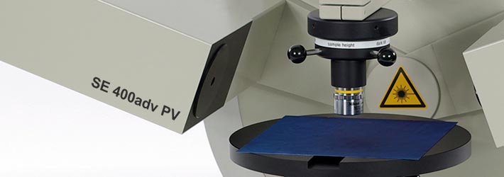
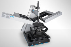
SENTECH Instruments develops, manufactures, and sells worldwide advanced quality instrumentation for Plasma Etching, PECVD, Atomic Layer Deposition, Thin Film Measurement (Spectroscopic Ellipsometry, Spectroscopic Reflectometry and Laser Ellipsometer) and Photovoltaics.
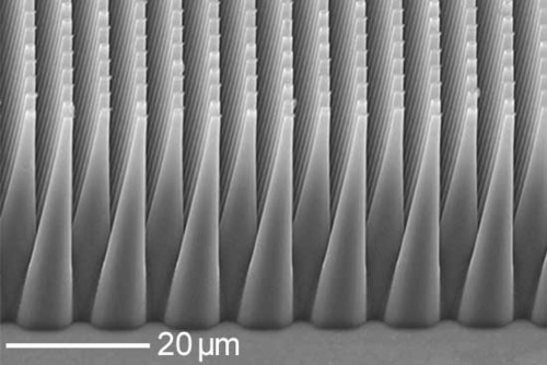
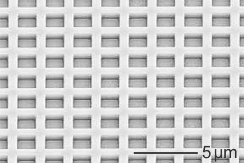
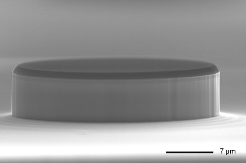
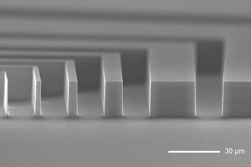
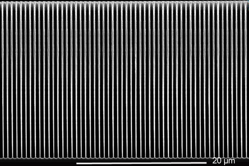
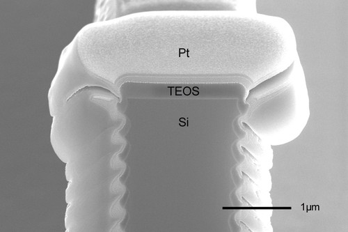
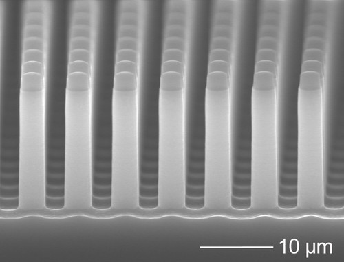
ICP-RIE Plasma Etching:
What's New?
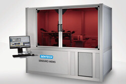
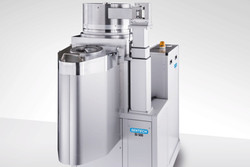
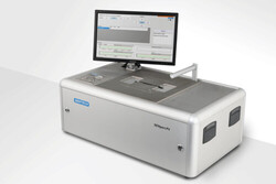
SENTECH proudly presents the SENDURO®MEMS for fully automatic metrology quality control in sensor and MEMS production. The SENDURO®MEMS provides reliable and precise measurement of thin film stacks, using spectroscopic reflectometry and ellipsometry. The SENDURO®MEMS equipped with reflectometer is for fast thin film measurement. →read more
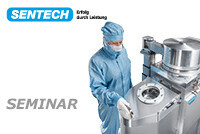
SENTECH offers an application oriented seminar “Plasma-Process-Technology” on April 7, 2022 at SENTECH in Berlin-Adlershof. Applications for low damage etching and deposition will be presented in sensors, quantum and III-V-devices. →read more
Upcoming Events:

SENTECH
Gesellschaft für Sensortechnik mbH
Konrad-Zuse-Bogen 13
82152 Krailling / KIM
Germany
Phone: +49 (0)89 - 89 79 60 70
Fax: +49 (0)89 - 89 79 60 722
Email: sales@sentech.de
| We hire! »Local Sales Manager« Apply here! |